KiCad zone not filling, or filling wrong: out-of-date fills, priority, thermal reliefs and islands
A copper zone in KiCad is an outline plus a fill, and the fill is a snapshot KiCad computes when you ask it to. Most zone problems come from that snapshot: it is older than the board, two zones disagree about who owns an area, a pad cannot be reached by enough spokes, or a keepout leaves a piece of copper on its own. Each case below was built on a real KiCad 9 board and run through KiCad’s own design rules check.
Last reviewed
Short answer
Press B (Edit → Fill All Zones) after any change, and tick “Refill all zones before performing DRC”: a stale fill shows up as clearance and solder mask errors that vanish on refill. If two pours overlap, give the one that should win a higher priority; at equal priority the winner is not yours to choose, and DRC does not complain. A “Thermal relief connection to zone incomplete” error means fewer spokes reach the pad than the zone requires (two by default). “Missing connection between items” between two pieces of the same zone means a keepout or a track cut the pour in two: join the pieces with a via or a track.
“Zone fills are out of date”: the fill is a snapshot
KiCad does not refill zones as you work. It fills them when you press B (Edit → Fill All Zones), when DRC runs with “Refill all zones before performing DRC” ticked, or when it asks “Zone fills are out-of-date. Refill?” and you say yes. Between those moments, the copper you see is whatever was filled last.
To see what that costs, the test board was filled, then the decoupling capacitor C1 was moved 2 mm and the board saved without refilling. KiCad 9.0.9’s DRC on that file:
[clearance]: Clearance violation (zone clearance 0.3000 mm; actual 0.0000 mm)
    @(123.2250 mm, 103.0000 mm): Pad 1 [+3V3] of C1 on F.Cu
    @(100.4000 mm, 100.4000 mm): Zone [GND] on F.Cu, priority 0
[solder_mask_bridge]: Front solder mask aperture bridges items with different nets
    @(123.2250 mm, 103.0000 mm): Pad 1 [+3V3] of C1 on F.Cu
    @(100.4000 mm, 100.4000 mm): Zone [GND] on F.Cu, priority 0
[track_dangling]: Track has unconnected end
    @(105.0000 mm, 105.0000 mm): Track [+3V3] on F.Cu, length 18.2250 mm
** Found 1 unconnected pads **
The first two errors are the old fill: the ground pour still has copper where C1’s +3V3 pad now sits. After a refill both disappear, and what remains is the real problem, the +3V3 track that still ends where C1 used to be. Refill first, then read the report; a stale fill hides real errors behind false ones.
Gerbers come from the saved fill too
Running DRC from the command line
In a script or CI job, kicad-cli pcb drc checks the board as saved. Version 9.0.9 has no option to refill first, so the stale board above fails the same way on the command line. Refill with pcbnew’s Python API before the check:
import sys, pcbnew
b = pcbnew.LoadBoard(sys.argv[1])
pcbnew.ZONE_FILLER(b).Fill(b.Zones())
pcbnew.SaveBoard(sys.argv[1], b)
That is the script used for every board on this page, and running it on the stale board cleared the two fill errors.
Two pours over one area: zone priority
A common layout puts a +3V3 pour over part of the board and a ground pour over all of it. Where they overlap, KiCad fills the higher-priority zone first and makes the other flow around it. With both at the default priority, nothing says which comes first.
The test board was built ten times from the same script, with a +3V3 pour over the left half and a ground pour over the whole board, both at priority 0. In seven builds +3V3 filled its half (246.5 mm²). In three, the ground pour took the overlap and +3V3 was left with 4.8 mm². DRC reported 0 violations on both outcomes: neither is a rule error, so nothing tells you which one you got.
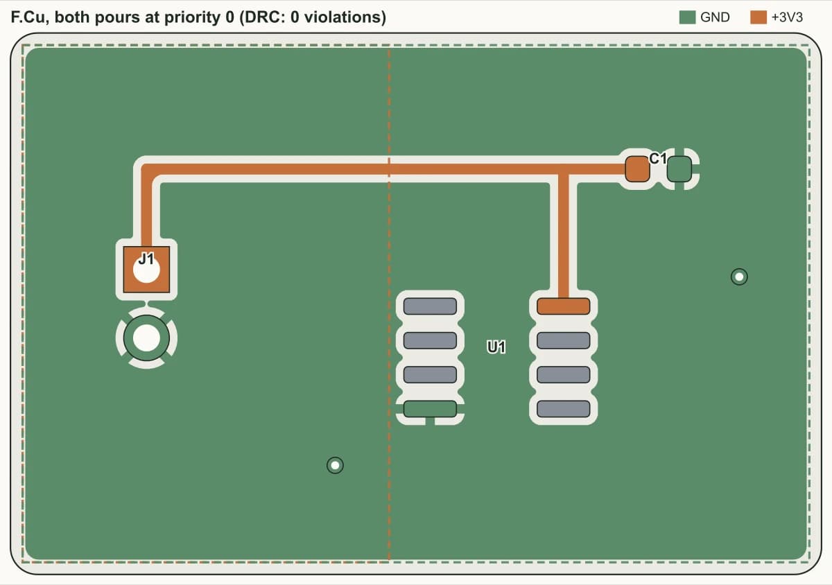
Setting the +3V3 pour to priority 1 made the result the same on every build:
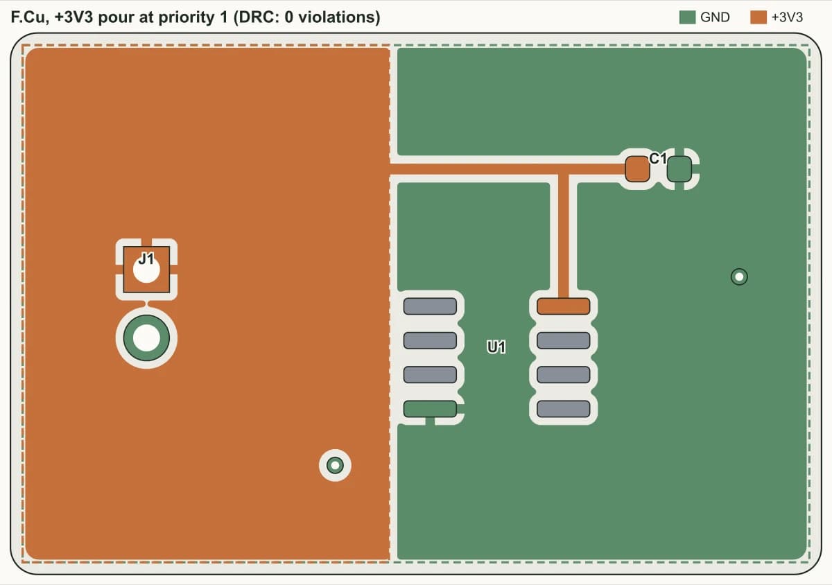
Set priority in the Zone Manager, which lists every zone in priority order and moves a zone up or down. Any two zones of different nets that overlap on one layer should have different priorities. Then refill and look at the result layer by layer.
“Thermal relief connection to zone incomplete”
A pad in a pour normally joins it through thermal relief spokes: a gap around the pad, bridged by narrow copper, so the pad can be soldered without the pour soaking up the heat. KiCad checks that enough spokes actually reach copper. By default a zone requires two.
On the test board, a no-fill area around the header’s ground pad leaves only one way in. KiCad 9.0.9 reports it on both layers:
[starved_thermal]: Thermal relief connection to zone incomplete (layer F.Cu; zone min spoke count 2; actual 1)
    @(100.4000 mm, 100.4000 mm): Zone [GND] on F.Cu, priority 0
    @(105.0000 mm, 111.2700 mm): PTH pad 2 [GND] of J1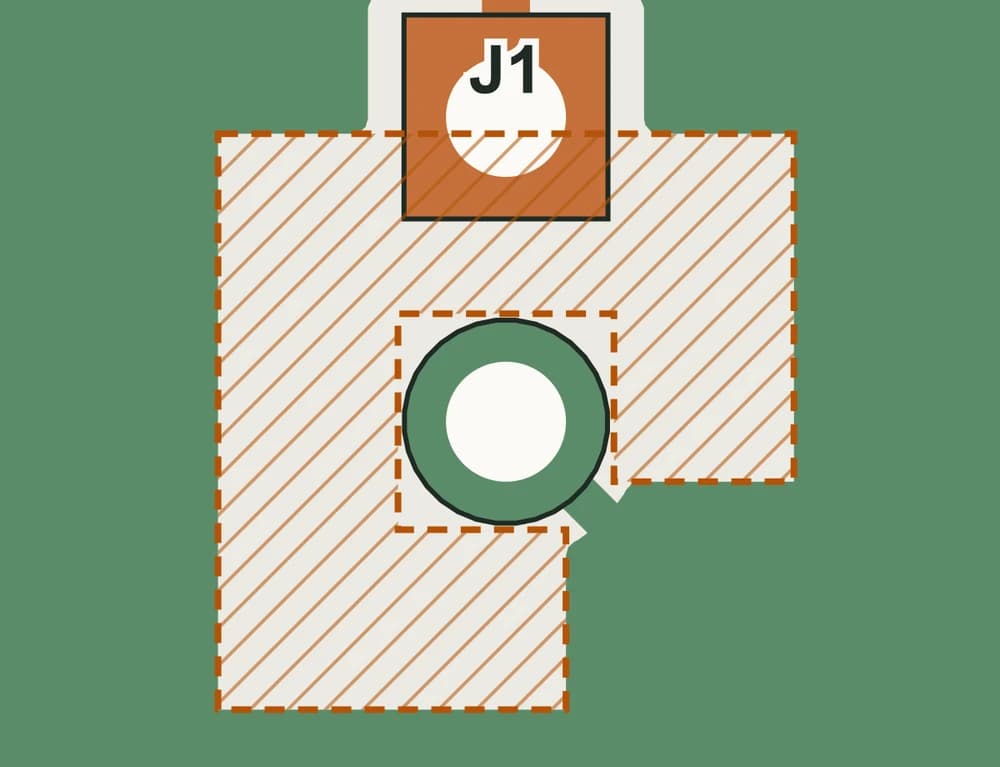
The pad is still connected, so this is not an open circuit; it is a weak joint and, with one spoke, one crack away from becoming one. Fixes, in order of preference:
- Move what blocks the spokes: a track squeezed past the pad, a keepout, a neighbouring pad’s clearance.
- Change the spoke angle so the spokes land where copper can reach.
- Narrow the thermal gap, within your fab’s clearance.
- Set that pad’s zone connection to solid. Fine for a pad that is easy to heat; harder to hand-solder on a large plane.
- Where one spoke is acceptable by design, a custom rule with the
min_resolved_spokesconstraint lowers the requirement for those pads only.
The KiCad forum threads behind this page are the same family: a pad that cannot reach a zone of its own net because a clearance rule leaves no room for spokes or copper. Find the rule DRC names, then decide whether the rule or the layout should give.
Islands, keepouts and “Missing connection between items”
A rule area (keepout) can forbid tracks, vias, pads, zone fills or footprints inside it. One that keeps out zone fills is how you keep copper away from an antenna or a mounting hole. It also splits pours. On the test board, an L-shaped band keeps fills out and cuts the top-right corner, with C1’s ground pad, away from the rest of the top pour:
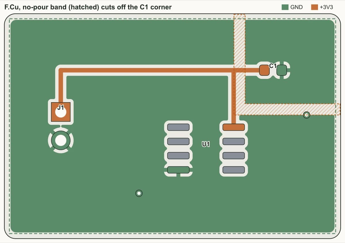
[unconnected_items]: Missing connection between items
    @(100.4000 mm, 100.4000 mm): Zone [GND] on F.Cu, priority 0
    @(100.4000 mm, 100.4000 mm): Zone [GND] on F.Cu, priority 0
“Missing connection between items”, naming the same zone twice, is the signature of a pour cut in two. The zone’s island setting decides what happens to pieces: Remove islands “Always”, “Never” or “Below area limit”. Here it was “Always”, yet the corner stayed, because C1’s ground pad sits on it; what is left is a real gap in the ground net. One via in the corner to the bottom pour joined the pieces, and DRC came back with 0 violations and 0 unconnected pads.
With island removal on, a piece that touches nothing of its net is deleted, which is why a zone can seem not to fill an area at all: the copper was there and was removed as an island. Add a via or a track into that area, or change the island setting, and refill.
When a zone will not fill at all
- Refill (B). A zone drawn after the last fill shows only its outline.
- Check the zone’s net. A zone on the wrong net, or on no net, never joins the pads you meant.
- Check its layer. A pour drawn on one copper layer does nothing on the other.
- Look for a higher-priority zone or a keepout over the same area.
- Check clearance and minimum width. A large zone clearance plus a minimum width that does not fit between pads leaves no copper in dense areas.
- Check the island setting, and whether the area has anything of the zone’s net in it.
How PCBEditor checks its pours
When PCBEditor routes a board with ground pours, its rules check reads the actual pour shapes rather than the outlines. It joins pads through traces, vias and the filled copper, then reports a net whose pads end up in separate pieces, with the pads left unreached and how many pieces there are. A pour piece that reaches no pad of its net is reported as isolated copper, and pour-to-copper clearance is checked like any other clearance.
It does not count thermal relief spokes, so a pad joined by a single spoke passes there. If you finish the board in KiCad, KiCad’s check is the one to read for thermal reliefs; the Gerber checklist covers what to look at before ordering.
Common questions
- Why is my KiCad zone not filling?
- Usually the fill is out of date (press B, Edit → Fill All Zones), the zone has no net or the wrong net, a higher-priority zone or a keepout covers the area, the clearance and minimum width leave no room for copper, or island removal deleted pieces that connect to nothing. Refill, then check the zone's net, priority, clearance and island setting.
- What does “Zone fills are out of date” mean in KiCad?
- Something changed on the board after the zones were last filled, so the saved fill no longer matches the parts and tracks, and KiCad can ask “Zone fills are out-of-date. Refill?”. Refill with B before running DRC or plotting Gerbers; a stale fill gives clearance and solder mask errors that are not real.
- How do I set zone priority in KiCad 9?
- In the Zone Manager, which lists the board's zones in priority order and moves a zone up or down. A higher-priority zone fills first and lower-priority zones flow around it with their clearance. Give every pair of overlapping zones on different nets different priorities.
- How do I fix “Thermal relief connection to zone incomplete”?
- Fewer thermal spokes reach the pad than the zone requires, two by default. Move whatever blocks the spokes (a track, a keepout, another pad), widen the space around the pad, change the spoke angle, or set that pad's zone connection to solid. A custom rule using the min_resolved_spokes constraint can lower the requirement where one spoke is acceptable.
- What is a keepout area in KiCad?
- A rule area that forbids items inside it: tracks, vias, pads, zone fills or footprints, each ticked separately (Keep out tracks, Keep out vias, Keep out pads, Keep out zone fills, Keep out footprints). One that keeps out zone fills is how you stop a pour under an antenna, but it can also cut a pour into islands.
- Does kicad-cli refill zones before DRC?
- kicad-cli 9.0.9's pcb drc has no refill option; it checks the fill saved in the file. Refill in a script with pcbnew's ZONE_FILLER first, or save the board after pressing B, so the command-line check sees current copper.
Let PCBEditor pour and check the ground plane
The editor opens with this board described in the chat box, ground pours included. Its rules check reads the filled copper and reports a net left in pieces or a pour that reaches no pad before you export.
Open the board in the editor→Sources
DRC reports are kicad-cli’s text output with the rule-source lines removed. Fill areas are read from the zones KiCad filled and saved; the figures are drawn from those polygons.
- KiCad 9.0.9 kicad-cli pcb drc, run on the seven test boards described on this page (built with the pcbnew Python API: a 30 × 20 mm 2-layer board with a 1×02 header, an SOIC-8 and an 0603 capacitor, ground pours on both layers).
- KiCad 9.0.9 pcbnew: dialog and message text (Refill all zones before performing DRC; Zone fills are out-of-date. Refill?; Remove islands: Always, Never, Below area limit; Keep out tracks, vias, pads, zone fills, footprints; Zone Manager) and the min_resolved_spokes custom rule constraint.
- KiCad 9.0 PCB Editor manual (docs.kicad.org): zones, zone priority, thermal reliefs, rule areas and custom design rules.
- KiCad forum, November 2026: “Which clearance rule is stopping pad 28 from reaching Vdd-zone?” and “Issue #24443 - DRC errors with pad close to a zone with the same net”.