Via-in-pad: when it’s safe, when it ruins a joint, and what to ask your fab
Putting a via straight into an SMD pad saves space and shortens the path to the next layer. On some boards it is the only way to route at all. Done carelessly, it drains solder out of the joint during reflow and leaves you with intermittent connections you can’t see. Whether it is safe comes down to one question: what happens to the hole.
Last reviewed
Short answer
Avoid open vias in small SMD pads: solder wicks down the hole and starves the joint. If there is room, put the via beside the pad on a short trace (a dog-bone). When you do need via-in-pad (fine-pitch BGAs, boxed-in pads), order the vias filled and plated over, IPC-4761 Type VII, often called VIPPO. Thermal vias in a QFN’s exposed pad are a common, accepted exception if you follow the part’s land-pattern guidance.
What via-in-pad means
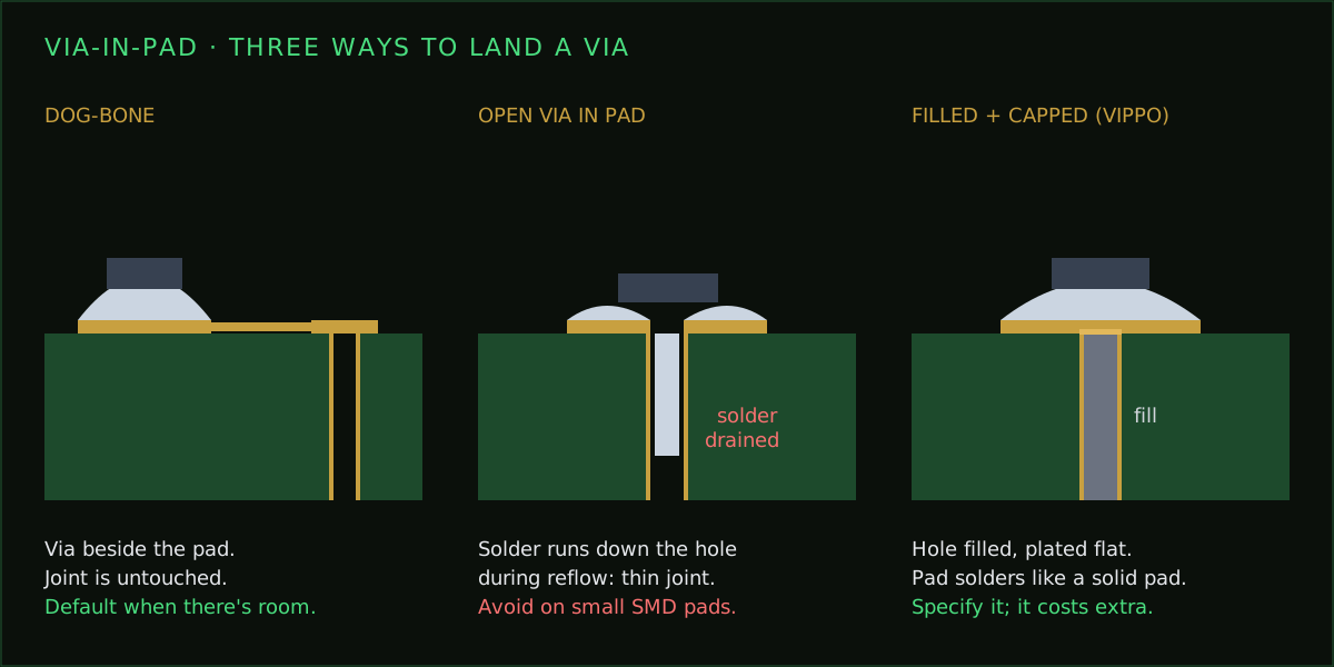
Normally a via sits a little away from the pad it serves, joined by a short trace. Seen from above, pad, trace and via look like a dog bone, hence the name. Via-in-pad drops the trace and drills the via through the pad itself. It saves the space the trace and via would take beside the pad and makes the connection to the next layer as short as it can be.
Why an open via in a pad fails
A plated hole is a capillary. During reflow, molten solder on the pad flows into the hole and down the barrel. The joint above is left with less solder than the paste stencil gave it. On a larger pad that might mean a weaker joint; on a small passive or a fine-pitch lead it can mean almost no joint at all. Solder can also come out on the other side of the board and form a bump that stops the board sitting flat.
The tombstone that started in the drill file
When via-in-pad is the right call
- Fine-pitch BGAs. Between tightly spaced balls there is no room for a via and a trace, so the inner balls go down through vias in their pads. These must be filled and capped.
- Boxed-in pads. On some dense packages the inner pads are surrounded by other pads with no path out on the top layer. A via in the pad is the only exit.
- Thermal pads. The exposed pad under a QFN or a power part is usually stitched to inner ground planes with an array of vias to carry heat away. This is normal; keep the drills small and follow the part’s recommended land pattern so not too much solder is lost.
- Very short high-speed or RF connections. Removing the dog-bone trace removes a little inductance, which matters at high frequencies.
IPC-4761: the fill types to ask for
IPC-4761 names seven ways to protect a via. Only the last one gives you a flat, plated pad that is safe to solder on, and it is what to write in your fab notes for via-in-pad.
| Type | Name | What it is |
|---|---|---|
| Type I | Tented | Dry-film mask laid over the hole, not filling it |
| Type II | Tented and covered | Tented, then covered with solder mask |
| Type III | Plugged | Hole partly filled with a non-conductive material |
| Type IV | Plugged and covered | Plugged, then covered with solder mask |
| Type V | Filled | Hole fully filled, conductive or non-conductive |
| Type VI | Filled and covered | Filled, then covered with solder mask |
| Type VII | Filled and capped | Filled, planarised and plated over: the one for via-in-pad |
Tenting and plugging (types I to IV) are for ordinary vias that are not in a pad: they stop solder mask gaps and keep solder or flux out of the hole. They are not a substitute for filling a via that sits under a solder joint.
What it costs, and who can build it
Filled and capped vias need extra steps: filling the hole, curing, sanding the surface flat and plating over it. That adds cost and often lead time, and some low-cost fabs don’t offer it at all or only on multilayer boards. Check your fab’s options before you lay out a board that depends on via-in-pad, and put the requirement in the fabrication notes so it is not missed.
A quick decision list
- Is there room for a via beside the pad on a short trace? Use a dog-bone.
- Is it a thermal pad under a QFN or power part? Thermal vias in the pad are normal; follow the land pattern.
- Is it a fine-pitch BGA or a boxed-in pad? Use via-in-pad, filled and capped (Type VII), and tell the fab.
- Is it a small passive or an ordinary fine-pitch lead? Don’t put an open via in it.
The via itself still needs a sensible size. The via and pad size calculator checks the drill against your board thickness, and the via current calculator shows how many you need for a power connection.
How PCBEditor uses it
PCBEditor’s router escapes dense parts with ordinary vias on short traces wherever there is a path. Only when a pad on a fine-pitch part is boxed in, with no route out on its own layer, does it launch that pad through a via in its centre, choosing the smallest via class that fits. In Review mode it asks before applying that rule. If your board ends up with signal vias in pads, order them filled and capped.
Common questions
- Is it OK to put a via in an SMD pad?
- Only if the via is filled and plated over (IPC-4761 Type VII, VIPPO), or for thermal vias in an exposed pad where the land-pattern guidance allows it. An open via in a small SMD pad drains solder from the joint.
- What is VIPPO?
- Via-in-pad plated over: the via is filled, planarised flat and plated with copper, so the pad solders like a solid pad. It is IPC-4761 Type VII and costs more than a standard via.
- Can I put vias in a QFN thermal pad?
- Yes, it is common practice, because the vias carry heat into the inner planes. Follow the part's recommended land pattern and IPC-7093 guidance on via size and count; small drills, tenting the far side or filling reduce how much solder wicks away.
- Does via-in-pad cost more?
- Filled and capped vias add fill, planarisation and plating steps, so they cost more and can add lead time. Not every budget fab offers them, so check before you design around them.
- Why use a dog-bone instead of via-in-pad?
- A short trace from the pad to a via beside it keeps the hole away from the solder joint, needs no special fab process and is cheaper. Use it whenever there is room.
Route fine-pitch parts without guessing
PCBEditor escapes dense parts with standard vias where it can, uses via-in-pad only for pads that are boxed in, and tells you when it does so you can order the right via fill.
Design a fine-pitch board→Sources
- IPC-4761: Design Guide for Protection of Printed Board Via Structures (via types I to VII).
- IPC-7093: Design and Assembly Process Implementation for Bottom Termination Components (thermal vias in exposed pads).
- IPC-7095: Design and Assembly Process Implementation for BGAs.