AI PCB design in practice: six boards from prompt to Gerbers, reviewed pin by pin
On 17 October 2026 we generated six boards on PCBEditor, each from one plain-English prompt: an ESP32-C3 sensor board, a USB-C LiPo charger, a 555 flasher, an Arduino Nano motor driver, an RP2040 board and an I²C OLED board. Then we reviewed every one against its datasheets. Here is what the AI got right, what we had to fix, and the board it could not finish.
Last reviewed
Short answer
AI PCB design means describing a board in plain language and getting back a schematic, placed and routed copper, a design-rule check and fab files. In our test, 5 of 6 boards ended fully routed with 0 DRC errors and exported Gerbers, but only 1 was correct as first generated; the rest needed a review and one or two chat edits each. The sixth, a 4-layer RP2040 board, did not finish routing. The AI drafts the board quickly; a review still decides whether it works.
What AI PCB design does
An AI PCB tool turns a description into a board. In PCBEditor one prompt gives you parts that exist, a wired schematic, a placement, routed copper and a design-rule check, and you can change any of it by chat or by hand.
The output is an ordinary design: a schematic you can edit, a layout you can move parts and traces on, and standard files (Gerber, drill, BOM, pick-and-place, KiCad). The question is not whether it produces a board. It always does. The question is whether that board is right.
The six boards and how they came out
| Board | Parts | Layers, size | Chat edits | Final state |
|---|---|---|---|---|
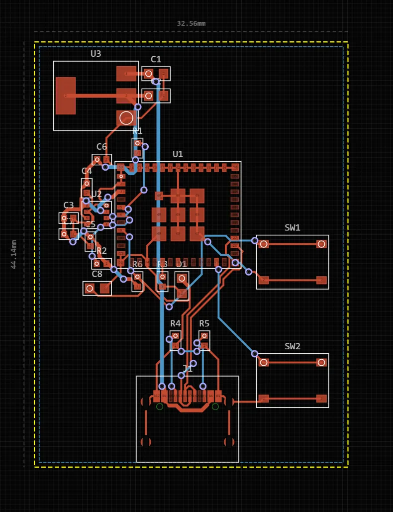
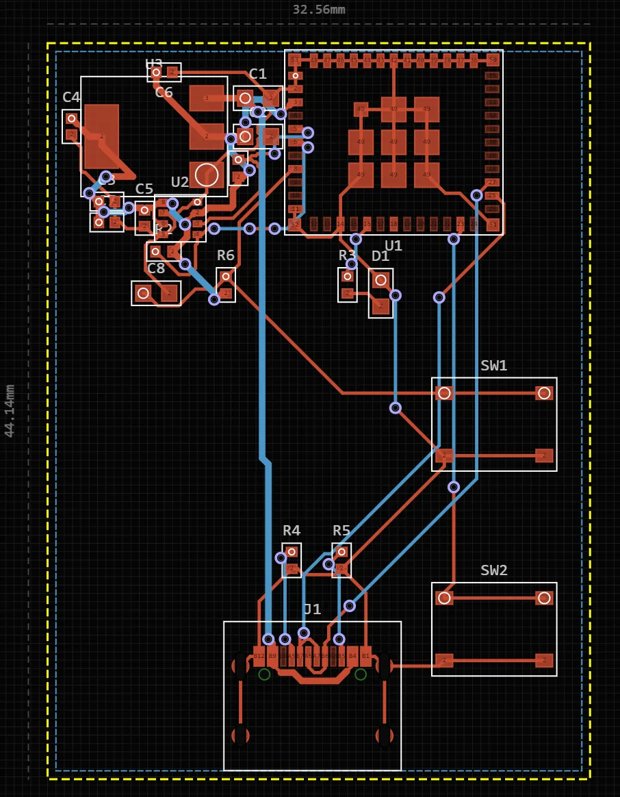
| ESP32-C3 sensor board | 21 | 2, 32.6 × 44.1 mm | 2 | All nets routed, 0 DRC errors, Gerbers exported |
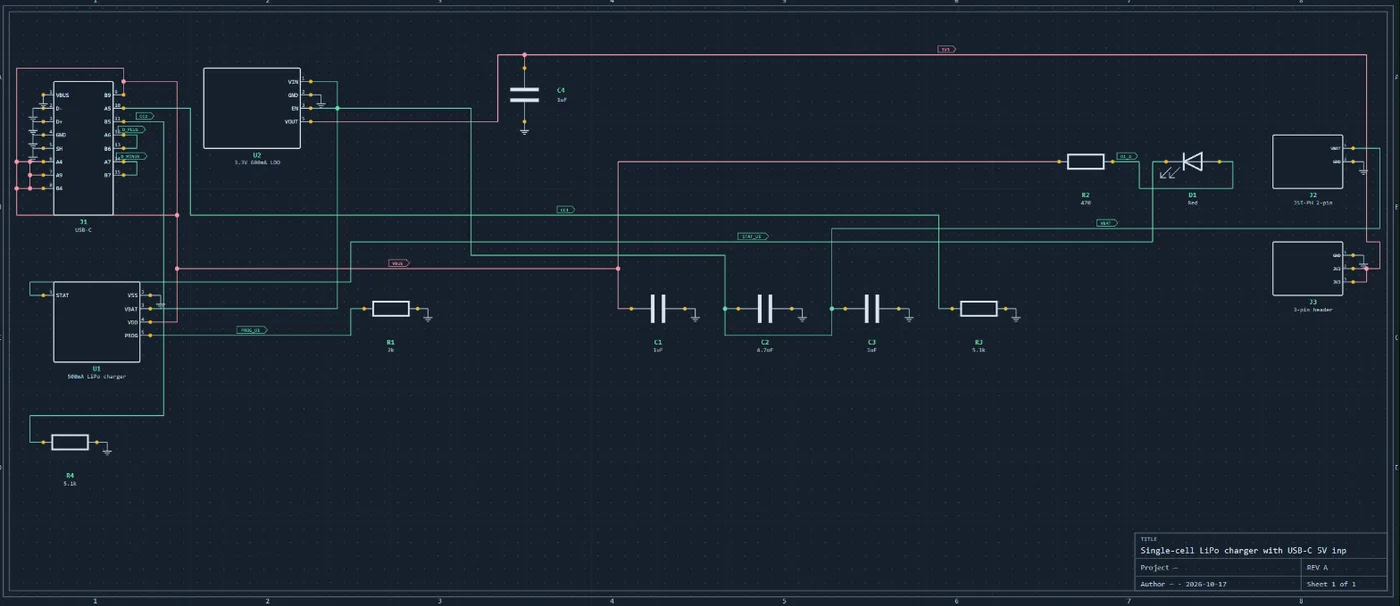
| USB-C LiPo charger | 14 | 2, 32.5 × 34.5 mm | 0 | All nets routed, 0 DRC errors, Gerbers exported |
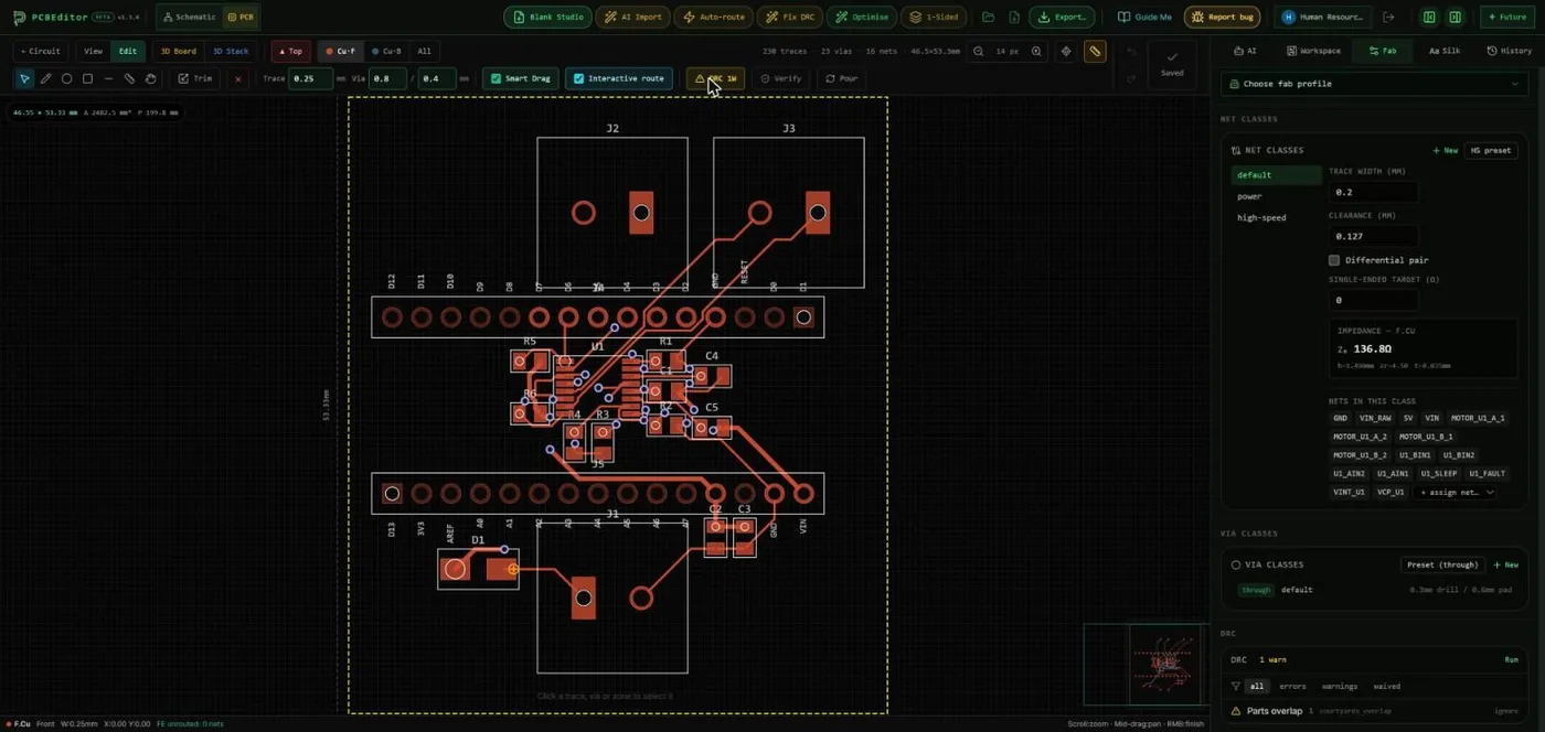
| Arduino Nano motor driver | 18 | 2, 46.5 × 53.3 mm | 1 | All nets routed, 0 DRC errors, Gerbers exported |
| I²C OLED board (ATtiny85) | 10 | 2, 31.5 × 26.6 mm | 2 | All nets routed, 0 DRC errors, Gerbers exported |
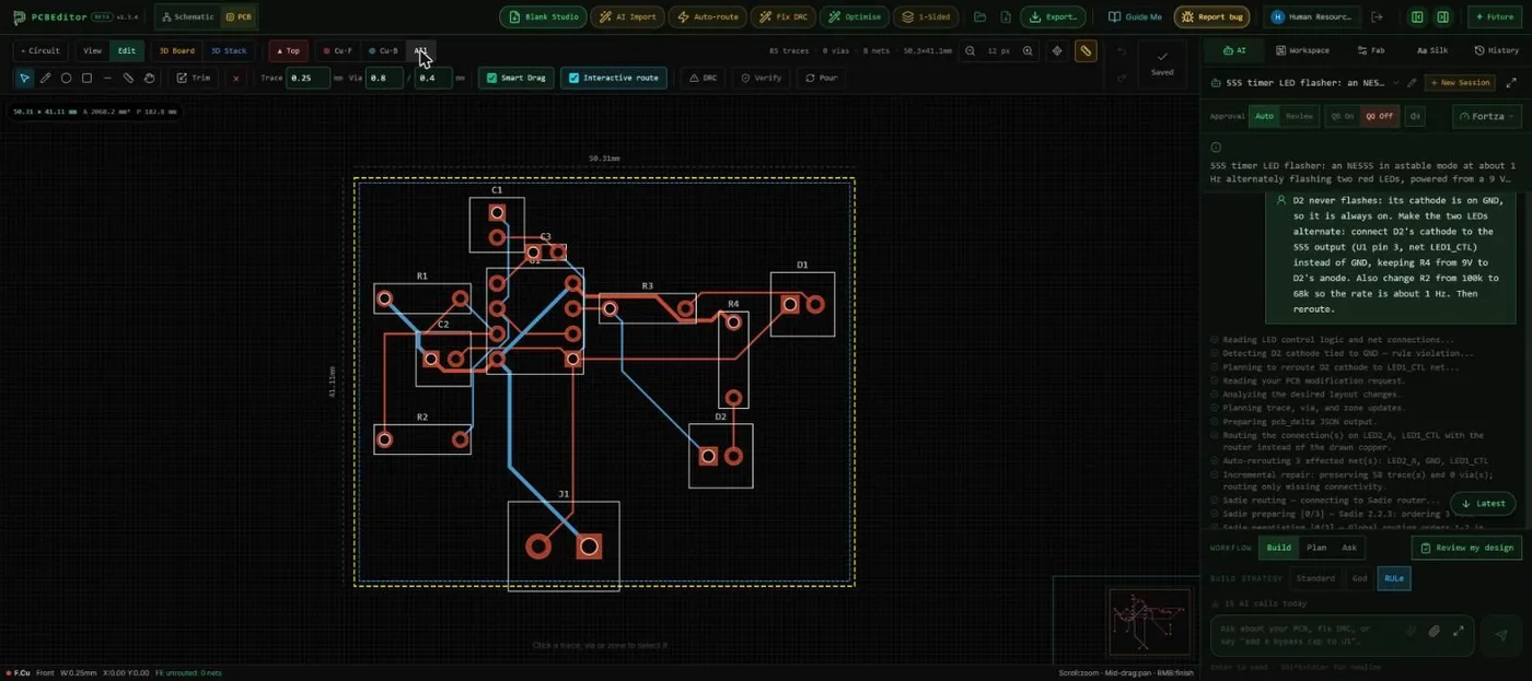
| 555 LED flasher | 11 | 2, 50.3 × 41.1 mm | 2 | All nets routed, 0 DRC errors, Gerbers exported |
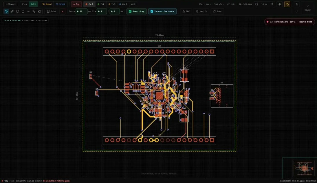
| RP2040 development board | 33 | 4, 70.2 × 50.8 mm | 2 | 9 nets unrouted, 2 DRC errors, Gerbers held back |
“Chat edits” counts the plain-English fix requests sent after the review. On the RP2040 board neither request changed the board: one was refused and one timed out.
- ESP32-C3 sensor board
Pin map correct against the ESP32-C3-MINI-1 datasheet: USB on GPIO18/19, BOOT on GPIO9, I2C on GPIO2/3 with 4.7 kΩ pull-ups, the BME280 strapped for I2C at address 0x76, 5.1 kΩ CC pull-downs on the USB-C port.
The "reset button" came out as a user button on GPIO4. One chat edit moved SW1 to EN, keeping the 10 kΩ pull-up and 1 µF capacitor.
The module sat mid-board with its antenna over parts and the bottom ground pour. A second chat edit moved it to the top edge so the antenna overhangs the board.
- USB-C LiPo charger
Correct on the first pass: 2 kΩ on PROG sets 500 mA, the charge LED sinks into STAT, the AP2112K runs from the battery with its enable tied high, and both CC pins have 5.1 kΩ pull-downs.
The run's regulator warning assumed a 5 V input, but the regulator runs from the battery (4.2 V at most), so the real worst-case dissipation is about 0.54 W, not 1 W.
- Arduino Nano motor driver
DRV8833 pin map correct, with the 10 nF charge-pump capacitor, 10 µF bulk on VM, a Schottky in series for reverse polarity, and pull-ups on nSLEEP and nFAULT.
The Nano's VIN pin was left unconnected although the prompt asked for it, and VINT had 1 µF where the datasheet asks for 2.2 µF. One chat edit fixed both.
The DRV8833 is rated for 10.8 V on VM, so the 12 V end of the requested supply is too high. The tool did not flag it; run this board from 10 V or less.
- I²C OLED board (ATtiny85)
SCL was on PB1, but the ATtiny85's I2C hardware needs it on PB2; the USB connector was not wired, so nothing powered the board; and a second 4-pin header duplicated the OLED socket.
One chat edit fixed all three but took MISO off the ISP header, and a second edit put it back. Always re-check the whole board after an edit.
- 555 LED flasher
The 555 itself was wired correctly, but the second LED had its cathode on ground, so it stayed lit instead of alternating. A chat edit moved it to the 555's output.
10 kΩ, 100 kΩ and 10 µF give 0.69 Hz, not about 1 Hz; the same edit changed 100 kΩ to 68 kΩ (0.99 Hz). A second edit added the 10 nF capacitor on pin 5 that the datasheet recommends.
- RP2040 development board
The circuit is right where it is wired: QSPI flash mapping, crystal, SWD, BOOTSEL through 1 kΩ on the flash chip-select (as on the Pico), 27 Ω USB series resistors, the core regulator and its capacitors.
GPIO26 to GPIO29 were left unconnected because the part check did not recognise their ADC-suffixed pin names, 9 nets stayed unrouted on four layers, and two DRC errors remained.
A chat edit to connect GPIO26 to GPIO29 was discarded rather than break the existing routing. The export held back the Gerbers. This board is not ready to order.
The walkthrough, step by step
1. Describe the board, with the numbers that matter
Each board started from one prompt typed into the editor. The prompts that worked best name the parts you already know you want (MCP73831, DRV8833, ESP32-C3-MINI-1), the interfaces (USB-C, I²C), the values that set behaviour (500 mA, about 1 Hz) and the layer count. Anything you leave out is chosen for you.
For example, the LiPo charger prompt was: “Single-cell LiPo charger board: USB-C 5 V input, MCP73831 charger set to 500 mA, a charge status LED, a JST-PH 2-pin battery connector, and an AP2112K 3.3 V regulator output on a 3-pin header. 2-layer board.”
2. Read the run log, not just the result
Every run shows what it decided: which footprint each part uses, which pins it left open rather than guess, and which nets did not route. On the 555 flasher it flagged pin 5 (CONT) as open; on the RP2040 board it listed every unrouted net by name. Those lines are where your review starts.
3. Review the schematic against the datasheets
This is the step that decides whether the board works. We checked every board pin by pin against its datasheets. One board (the LiPo charger) passed as generated. The others had at least one real mistake, and none of them would have shown up in a design-rule check:
- The ESP32-C3 board’s “reset button” was a user button on GPIO4, with nothing on EN.
- The 555 flasher’s second LED had its cathode on ground, so it never flashed.
- The Nano motor driver left the Nano’s VIN pin unconnected, although the prompt asked for it.
- The ATtiny85 board had SCL on PB1 (the chip’s I²C hardware needs PB2) and an unwired USB connector.
4. Fix it in plain English, then check the fix
Each mistake was fixed with one chat message that named the pins, for example “connect D2’s cathode to the 555 output (U1 pin 3) instead of GND”. The editor reroutes only the nets that changed and keeps the rest of the copper. Check every edit: on the ATtiny85 board, the edit that fixed SCL also took MISO off the programming header, and it took a second message to put it back.
5. Look at the layout as well as the netlist
A correct netlist can still be a bad board. The ESP32-C3 module’s antenna is the end beyond its top row of pads, and Espressif asks for it to sit at the board edge with no copper under it. The first layout put the module in the middle, over a ground pour, and it passed DRC. One chat message moved the module to the edge.
6. Run the design-rule check and look in 3D
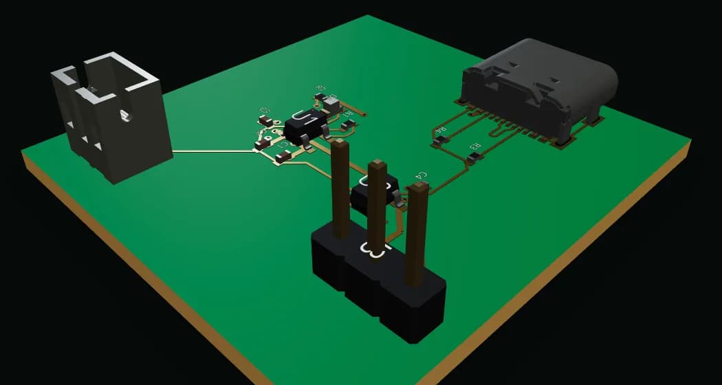
The design-rule check runs against the board’s own trace, clearance and drill rules. Five of the six boards finished with 0 errors and every net routed. The 3D view is for the things DRC does not check: which way a connector faces, and whether a part has a real model or a placeholder box.
7. Export and check the files
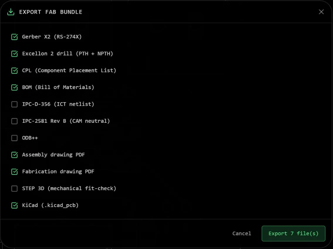
One dialog exports Gerber X2, Excellon drill, pick-and-place, BOM, IPC-D-356, IPC-2581, ODB++, assembly and fabrication PDFs, STEP and a KiCad board. While a board still has DRC errors, the export holds back the fab files, as it did for the RP2040 board. Before ordering, open the zip in a Gerber viewer and go through the Gerber checklist.
Where it failed
The RP2040 board is the honest limit of this test. It asked for a 7 × 7 mm QFN-56 at 0.4 mm pitch, QSPI flash, a crystal, USB-C, a regulator and two 20-pin headers on four layers. The circuit was right where it was wired, but four ADC pins (GPIO26 to GPIO29) were left unconnected, 9 of 47 nets did not route, and 2 DRC errors remained. When we asked for the four missing connections, the editor refused the change rather than break existing routes, and the export held back the Gerbers.
A clean DRC is not a working board
A review checklist for any AI-generated board
Run Review my design first: it covers the design rules and the electrical faults the checks can catch (how it works: AI PCB review). Then go through what only a person can judge:
- Follow power from the connector to every IC: input protection, regulator input and output, enable pins.
- Check every reset, boot and enable strap, with its pull-up or pull-down and capacitor.
- Check pins with special functions against the datasheet: I²C, SPI, ADC, USB, crystal, programming header.
- Compare every supply with every part’s rating (absolute maximum, not typical).
- Check the datasheet’s required capacitors: values, not just presence.
- Look at the layout: antenna keepouts, connectors on the edge facing out, decoupling next to its pins.
- After every chat edit, export again and re-check the pins it touched and their neighbours.
Is it an AI PCB designer?
It does the drafting a PCB designer does: finding parts, wiring symbols, placing footprints, routing and checking clearances, in minutes instead of an afternoon. It does not yet do the judgement. Across six boards, every mistake was caught by a person reading datasheets, and every fix was a sentence that person wrote. Treat it as a fast junior drafter whose work you check, not as a designer you can sign off on.
For the questions to ask any AI PCB tool before you trust it, see how to evaluate AI PCB software.
Can a chat assistant design a PCB?
A general assistant is good at choosing parts and explaining a topology, but it cannot place, route or design-rule-check a board. Here is where the line falls for each.
Common questions
- What is AI PCB design?
- AI PCB design is generating a circuit board from a description: you say what the board must do and get back the parts, a schematic, placed and routed copper, a design-rule check and the fab files. PCBEditor does all of that from one prompt, and you can change the result in plain language or by hand.
- Can AI design a PCB by itself?
- Not reliably yet. In our test of six boards generated on 17 October 2026, five finished fully routed with no DRC errors, but only one was electrically correct as first generated. The others had mistakes a design-rule check cannot see, such as a reset button on the wrong pin or an LED that could never flash, and needed a human review and a chat edit.
- Is there a free AI PCB designer?
- PCBEditor is free to use: describe a board, and it generates the schematic and a routed, DRC-checked layout, and exports Gerbers, drill files, BOM, pick-and-place and a KiCad board. AI generation needs a free account; the editor opens without one.
- What does PCB AI get wrong?
- In our six-board test, the mistakes were electrical intent, not geometry: a reset button wired to a GPIO, an LED wired permanently on, a power pin left unconnected, an I2C clock on a pin without I2C hardware, an antenna placed over a ground pour, and a 12 V supply on a driver rated for 10.8 V. Every one passed the design-rule check.
- Can AI route a 4-layer board?
- Smaller 4-layer boards, yes. Our 4-layer RP2040 board, a 7 × 7 mm QFN-56 at 0.4 mm pitch with QSPI flash and USB on 70 × 51 mm, finished with 9 of its 47 nets unrouted and 2 DRC errors, so it was not ready to order. Dense fine-pitch parts still need a person to guide placement.
- Does AI PCB design replace an electronics engineer?
- No. It removes the drafting: parts lookup, symbol and footprint wiring, placement and routing. Deciding whether the circuit is right, reading datasheets and checking the layout against them is still the engineer's job, and it is where every mistake in our test was caught.
Try it on your own board
Describe a board and review what comes back, using the checklist above. A free account unlocks AI generation.
Open the editor→Sources
Each board was generated on pcbeditor.com on 17 October 2026 with the default settings, and checked against the exported KiCad board, BOM and Gerbers.
- Espressif, ESP32-C3-MINI-1 datasheet: module dimensions and antenna placement on the base board.
- Texas Instruments, DRV8833 datasheet: VM 2.7-10.8 V recommended, 11.8 V absolute maximum; 0.01 µF VCP-to-VM and 2.2 µF VINT capacitors.
- Microchip, MCP73831/2 datasheet: charge current set by the PROG resistor (2 kΩ for 500 mA).
- Texas Instruments, NE555 datasheet: astable frequency 1.44 / ((RA + 2RB) C); 10 nF decoupling on CONT.
- Microchip, ATtiny25/45/85 datasheet: USI two-wire mode uses PB0 (SDA) and PB2 (SCL).
- Raspberry Pi, RP2040 datasheet: GPIO26-GPIO29 are ADC0-ADC3 on QFN-56 pins 38-41; hardware design guide for the QSPI flash and BOOTSEL circuit.
- USB Type-C specification: 5.1 kΩ Rd pull-downs on CC1 and CC2 for a power sink.