KiCad’s “Input Power pin not driven by any Output Power pins”: what it means and where PWR_FLAG goes
You draw a correct power supply, run the electrical rule check, and KiCad says your 5 V rail and your ground are not driven by anything. The schematic is usually fine. The check needs to be told where the power comes from, and the way to tell it is a PWR_FLAG. Put one in the wrong place, though, and you get a second error: “Pins of type Power output and Power output are connected”.
Last reviewed
Short answer
KiCad’s ERC wants every net that has a power input pin on it (a chip’s VCC or GND, a power symbol) to also have a power output pin, such as a regulator’s output. Power that arrives through a connector, a battery or a USB socket comes in on passive pins, so the check sees nothing driving the net. Place one PWR_FLAG (from the power library) on each such net, usually the input rail and GND, and nowhere else. A flag on a rail that a regulator already drives gives “Pins of type Power output and Power output are connected”; remove that flag.
Why KiCad says the pin is not driven
Every pin in a KiCad symbol has an electrical type: input, output, bidirectional, passive, power input, power output and a few more. The electrical rule check (ERC) uses those types to judge each net. One of its rules, in the words of KiCad’s manual: the violation occurs when a symbol pin with electrical type Input Power is not connected to an Output Power pin.
Power inputs are everywhere: the regulator’s VIN and GND, a microcontroller’s VDD, and every power symbol (+5V, +3V3, GND) is itself a single power input pin. Power outputs are much rarer; a regulator’s output is the usual one. The parts that bring power onto the board are passive. KiCad 9’s pin header, battery, barrel jack and USB-C VBUS pins are all passive, so as far as ERC knows, nothing drives the rail they feed.
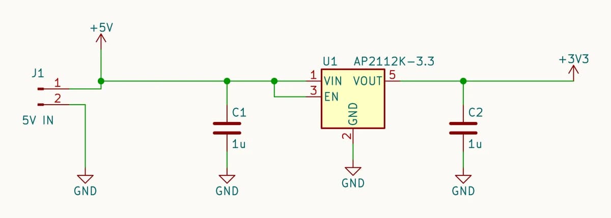
This is what KiCad 9.0.9 reports for that sheet:
[power_pin_not_driven]: Input Power pin not driven by any Output Power pins
    ; error
    @(38.10 mm, 55.88 mm): Symbol #PWR04 Pin 1 [Power input, Line]
[power_pin_not_driven]: Input Power pin not driven by any Output Power pins
    ; error
    @(78.74 mm, 73.66 mm): Symbol #PWR01 Pin 1 [Power input, Line]

 ** ERC messages: 2  Errors 2  Warnings 0
The error lands on one power symbol per net: #PWR04 is the +5V symbol and #PWR01 is a GND symbol. Nothing is reported for +3V3, because the AP2112K’s VOUT pin is typed power output in KiCad’s symbol and drives that net.
Why GND gets the error too
Nothing in KiCad’s library outputs ground. The regulator’s GND pin is a power input, the GND symbol is a power input, and the header pin that carries the return current is passive. So ground needs the same treatment as the input rail, which is why the error so often names GND on a board whose ground is plainly connected.
Symbols with invisible power pins, common in older libraries, can add the error to nets you never drew. KiCad connects an invisible power input pin to a global net with the pin’s name, so hidden VCC and GND pins put power inputs on VCC and GND whether or not your sheet uses those names.
The fix: one PWR_FLAG per externally fed net
PWR_FLAG is in KiCad’s power library. It is a symbol with one pin of type power output and nothing else: no part on the board, no footprint, no net of its own. Wire it to a net and that net now has a power output, so ERC accepts it. Connecting any other power output pin does the same.
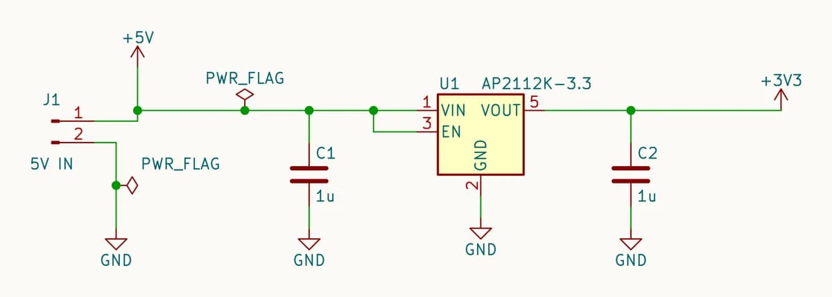
Where to put one:
- On the rail where power enters the board: the connector, battery, USB VBUS or barrel jack side.
- On GND.
- On a rail made through a passive part, if that rail has power inputs on it. Fuses, ferrite beads, diodes, resistors, and the drain and source of a MOSFET switch are passive in KiCad’s library, so a 3V3_FILT after a ferrite bead or a VBAT_SW after a P-MOSFET needs its own flag.
- Once per net. A second flag on the same net is a second power output, and KiCad reports the pair as an error.
Not on a regulator’s output
Editing the connector’s pin types to power output also silences the error, but every copy of that symbol then claims to be a supply, even where the connector carries signals or is a board’s output. A flag says it once, on the sheet where it is true.
When the error is real
The same check catches rails that really have no supply, which is why ignoring it or excluding every marker is a poor fix. Power symbols with the same value connect anywhere in the schematic, and symbols with different values never do. A +3.3V symbol on a sheet whose regulator feeds +3V3 makes two separate nets, and the misnamed one reaches only power inputs. ERC flags it; the board would have a chip with no supply.
It also catches a regulator whose output was never wired to the rail, and a rail you meant to feed from a second connector that never made it onto the sheet. Place the flags where power really enters, run ERC again, and read every error that is left.
“Pins of type Power output and Power output are connected”
This is the error people meet right after learning about PWR_FLAG. A flag is a power output, so a flag on a rail that a regulator drives puts two power outputs on one net, and KiCad’s default rules make that an error. Here is the report for the sheet above with a third flag added on +3V3:
[pin_to_pin]: Pins of type Power output and Power output are connected
    ; error
    @(104.14 mm, 60.96 mm): Symbol #FLG03 Pin 1 [Power output, Line]
    @(86.36 mm, 60.96 mm): Symbol U1 Pin 5 [VOUT, Power output, Line]
The fix is to remove the flag; the regulator already drives that rail. Two flags on the same net give the same error, so keep one.
The same message for two real parts is worth reading carefully. Two regulators with their outputs tied, the usual attempt at more current, get the same error, and this time it describes a real problem. Each regulator holds its own output voltage, and two parts never sit at exactly the same one, so the one a few millivolts higher supplies most of the current. Regulators share a load through ballast resistors in each output, as in TI’s application note on parallel LDOs, or through a part made for current sharing. Otherwise, use one regulator rated for the whole load.
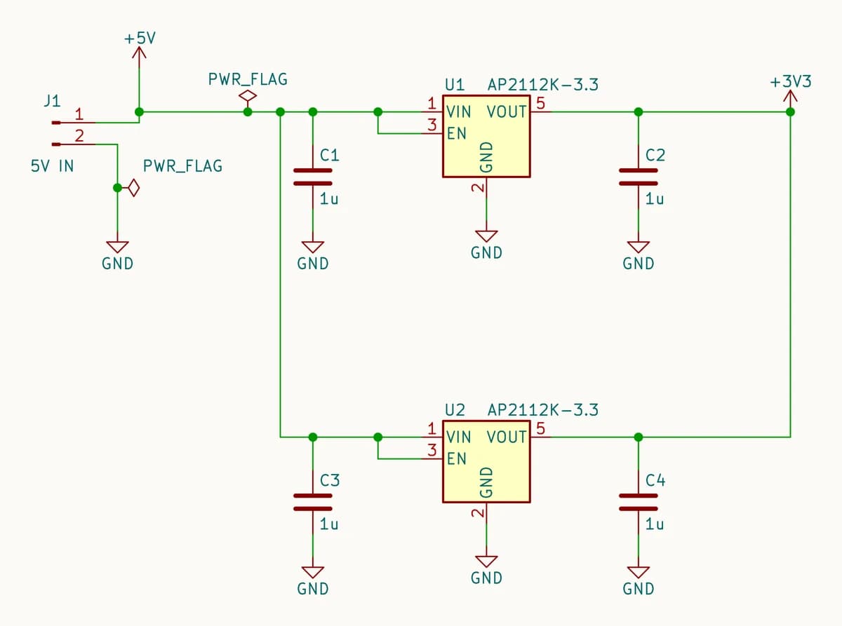
The other “Pins of type … are connected” messages
ERC judges every pair of pin types on a net against a pin conflict map, which you can see and change in the schematic setup. These are KiCad 9’s defaults for a power output pin, a regulator output or a PWR_FLAG, meeting each other type:
| Pin on the same net | KiCad 9 default | What it usually means |
|---|---|---|
| Power output | Error | Two regulators on one rail, or a PWR_FLAG on a rail a regulator already drives |
| Output | Error | A logic output wired to a supply rail |
| Tri-state | Error | A tri-state output on a supply rail |
| Open collector | Error | An open-collector output on a supply rail |
| Open emitter | Error | An open-emitter output on a supply rail |
| Bidirectional | Warning | A GPIO or I/O pin on a supply rail |
| Unspecified | Warning | A symbol whose pin type was never set |
| Input, passive, power input | No message | What a rail normally feeds |
When one of these appears, either the wire is wrong (a GPIO landed on a supply rail) or a symbol’s pin type is. Check the pin against the datasheet. If the symbol is wrong, fix it in your project library rather than relaxing the map: the map applies to every net in the design.
How PCBEditor checks power rails
PCBEditor’s electrical check, which runs on the boards it designs, asks the same two questions without flags. A rail that reaches only supply inputs and capacitors is reported as an error, “nothing supplies net …”, and pull-up resistors hanging off it do not count as a supply. A connector, a switch or a series part such as a fuse or ferrite counts as a possible source, so a board fed from a header passes without anything added.
Two supply outputs on one rail is an error too, and it counts a switching regulator that drives the rail through its inductor, which has no power output pin for a pin-type check to see. It is one of the faults that hold back the fab files until you have read it and confirmed. A dev-board module whose 3V3 pin is tied to the board’s own regulator gets a warning: with the module’s USB plugged in, that is two regulators on one rail. If you bring a KiCad schematic in, power symbols are read as net names and PWR_FLAG as a marker, never as parts on the board.
The limit is the same as KiCad’s: both checks read what each pin does from the part’s symbol. A linear regulator whose output pin is marked as something else would slip past both. Check regulator symbols against their datasheets, wherever you draw the schematic; the schematic symbols chart shows what each symbol stands for.
Common questions
- What does “Input Power pin not driven by any Output Power pins” mean in KiCad?
- A net has at least one pin whose electrical type is power input, such as a chip's VCC or GND pin or a power symbol, and no pin of type power output on it. KiCad cannot see a supply for that net. When the power really comes from a connector, a battery or a USB socket, whose pins are passive in KiCad's library, place a PWR_FLAG on the net.
- Where should I put PWR_FLAG in KiCad?
- On each net whose power comes from outside the sheet or through passive parts: the rail at the input connector or battery, GND, and any rail made through a fuse, ferrite bead, diode or transistor switch that has power input pins on it. Exactly one flag per net: two flags on one net are reported as an error. Never on a net a regulator's output already drives.
- Why does KiCad say GND is not driven?
- Nothing in KiCad's library outputs ground. Chips have GND pins of type power input, the GND symbol is a power input too, and the connector or battery that carries the return is passive. Ground needs a PWR_FLAG like the input rail does.
- Why do I get “Pins of type Power output and Power output are connected” after adding PWR_FLAG?
- PWR_FLAG is a power output pin. Put it on a rail that a regulator's output already drives and the net has two power outputs, which KiCad's default rules report as an error. Remove the flag from that rail. If two regulator outputs are tied together, the error is real: they will not share the load.
- Can I just ignore or exclude the power pin error?
- You can, but the same check catches real mistakes: a +3.3V power symbol on a sheet whose regulator feeds +3V3 makes two separate nets, and the misnamed one has no supply. Place PWR_FLAG where power really enters, and read every error that remains.
- Does a ferrite bead or fuse need its own PWR_FLAG?
- If the net after it has power input pins on it, yes. Fuses, ferrite beads, diodes and resistors have passive pins in KiCad's library, so a supply does not pass through them as far as ERC is concerned.
Try the same 5 V to 3.3 V board in PCBEditor
The editor opens with this circuit described in the chat box. Change it to your own; its electrical check reports a rail that nothing supplies and two regulators on one rail before any fab file is written.
Open the 5 V to 3.3 V board in the editor→Sources
The ERC reports are copied from kicad-cli’s text output; only the date line and sheet header are left out.
- KiCad 9.0 Schematic Editor manual (docs.kicad.org): the PWR_FLAG section, Power Symbols, Hidden Power Pins, and the electrical rules check entry “Input Power pin not driven by any Output Power pins” (default severity error).
- KiCad source, eeschema/erc/erc_settings.cpp on the 9.0 branch: the default pin conflict map (ERC_SETTINGS::m_defaultPinMap), the power-output row of which is the table above.
- KiCad 9.0.9 kicad-cli sch erc, run on the four schematics shown, and the pin types of the KiCad 9 symbol library (AP2112K-3.3, Conn_01x02_Pin, Battery, Fuse, FerriteBead, D, R, AO3401A, Barrel_Jack, USB-C receptacle, PWR_FLAG).
- Diodes Incorporated, AP2112 datasheet (DS39724 Rev. 2): typical application with 1 µF on the input and the output and EN tied to VIN.
- Texas Instruments, application note SBVA093 (December 2022): current sharing among parallel LDOs with ballast resistors.