How to create a symbol in KiCad 9, from datasheet to a clean ERC
Sooner or later you need a part KiCad doesn’t ship. Drawing the box takes five minutes. What decides whether the symbol helps or hurts is everything around it: which library it lives in, whether its pin numbers match the footprint, which electrical type each pin gets, and what happens to the thermal pad. This guide makes one real symbol, for TI’s BQ25185 LiPo charger, and checks every choice with KiCad 9’s own tools.
Last reviewed
Short answer
Open the Symbol Editor (Tools → Symbol Editor in the Schematic Editor). Make your own library with File → New Library… and choose the project table, so the library travels with the project. Select that library, then File → New Symbol…, and give it a name and a reference prefix such as U. Add one pin per pad: the number from the datasheet’s pin table and package drawing, the name, and an electrical type (power input for supply and ground pins, power output for rails the chip drives, input, output, open collector or passive for the rest). Run the symbol checker, save, place the symbol, and run ERC.
1. Make a library first
A KiCad symbol always lives in a library, a .kicad_sym file, and KiCad finds libraries through two tables: a global one, available to every project, and one per project, saved as sym-lib-table next to the project. Make your own library rather than adding to KiCad’s. In the Symbol Editor, File → New Library… asks which table to add it to, then where to save it.
Choose the project table when the parts belong to this design. The library file sits in the project folder, the table entry points at it with ${KIPRJMOD} (the project’s own folder), and the project still opens on another computer. Choose the global table for a library you will use in every project, and keep it somewhere you back up.
Two messages mean the library is in the wrong place:
- “Library ‘…’ is read-only. Choose a different library to save the symbol ‘…’ to.” You edited a symbol from one of KiCad’s own libraries, which are usually installed where you can’t write. Use File → Save As… and pick your library. “Symbol library ‘…’ is not writable.” means the same for a library file you lack permission to change.
- “The current configuration does not include the symbol library ‘…’”, an ERC warning. A symbol on the sheet came from a library that is in neither table, usually after copying a schematic from another project. Add the library under Preferences → Manage Symbol Libraries….
This is the second one, from the sheet built for this page before its library was listed in a table:
[lib_symbol_issues]: The current configuration does not include the symbol library 'my_parts'
    ; warning
    @(139.70 mm, 76.20 mm): Symbol U1 [BQ25185]
With the library listed in the project’s table, the same sheet reports 0 errors and 0 warnings.
2. Create the symbol
Select your library in the tree; a new symbol goes into the active library. Then File → New Symbol…. The dialog asks for:
- the symbol name (BQ25185 here) and the reference designator prefix, U for an IC;
- “Derive from existing symbol:”, for a part that shares another part’s pins and drawing (a different voltage option of the same chip, say). The base symbol has to be in the same library;
- “Number of units per package:” and “All units are interchangeable”, for parts like quad gates (below);
- “Create symbol with alternate body style (De Morgan)” and “Create symbol as power symbol”, both off for an IC;
- whether to exclude the part from the bill of materials or the board.
All of these can be changed later in Symbol Properties, but set the number of units now: it decides how the pins you add are shared between units.
3. Pins: numbers come from the package, not only the pin table
KiCad’s manual puts it plainly: symbol pins are matched to footprint pads by number. The name is for people; the number makes the connection. So every pad that carries a signal or a supply needs a pin with exactly its pad number, and pin numbers must be unique in a symbol (names may repeat).
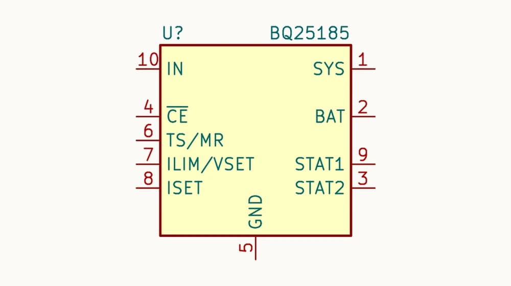
Take the numbers from the datasheet, and read the package drawing as well as the pin table. The BQ25185’s Table 4-1 lists ten pins. Its WSON-10 package has an eleventh pad, the thermal pad, which the table never mentions. TI’s package outline numbers it 11, and the layout section says the ground plane must be tied to the GND pin and the thermal pad. A symbol drawn from the pin table alone has no pin 11, so pad 11 of the footprint would get no net.
A few rules that save trouble later:
- No spaces in names or numbers. KiCad replaces them with underscores. Slashes are fine: TS/MR and ILIM/VSET are names exactly as TI prints them.
- Active-low names use a tilde and braces:
~{CE}draws CE with a bar over it. - Keep pin ends on the grid. KiCad’s own symbols put pins 2.54 mm (100 mil) apart. A pin end off the schematic’s connection grid is hard to wire, and ERC reports it as “Symbol pin or wire end off connection grid”.
- Inputs on the left, outputs on the right, supply at the top, ground at the bottom, as KiCad’s library does.
4. Pick each pin’s electrical type
The electrical type is what ERC reads. Get it wrong and ERC either cries wolf or keeps quiet about a real fault. KiCad 9 has twelve types: input, output, bidirectional, tri-state, passive, free, unspecified, power input, power output, open collector, open emitter and unconnected. Datasheets use a coarser scheme. TI’s table gives P, I, O and I/O, so the KiCad type is your decision. These are the BQ25185’s pins:
| Pin | Name | TI type | KiCad type | Why |
|---|---|---|---|---|
| 10 | IN | P | Power input | Supply in. A power input also tells ERC to look for a source on that net. |
| 5 | GND | — | Power input | Ground. KiCad's own charger symbols type GND this way. |
| 11 | GND | not in the table | Passive, hidden, stacked on pin 5 | The thermal pad. TI's package drawing numbers it 11. |
| 1 | SYS | P | Power output | The regulated system rail this chip drives. |
| 2 | BAT | P | Power output | Charges the cell. The battery connector is passive, so nothing conflicts. |
| 4 | ~{CE} | I | Input | Logic input, active low. Written ~{CE} so KiCad draws the bar. |
| 6 | TS/MR | I/O | Input | Thermistor or button input; it goes to a resistor, a thermistor or a switch. |
| 7 | ILIM/VSET | I/O | Passive | Only ever goes to a resistor to GND. |
| 8 | ISET | I/O | Passive | Same: a resistor sets the charge current. |
| 9 | STAT1 | O | Open collector | Open-drain status output: it only pulls low. |
| 3 | STAT2 | O | Open collector | Same as STAT1. |
These follow KiCad’s own symbol for the BQ24074, another TI charger with a power path. There, BAT and OUT are power outputs, ISET and ILIM are passive, the status pins are open collector, and the exposed pad is a hidden passive pin stacked on VSS. KiCad’s library is not fully consistent, though: its BQ25173 types ISET as an input. Both give no message when the pin goes to a resistor, because ERC counts a passive pin as something that drives an input.
KiCad’s manual goes further for pins like ISET, which push a current into a resistor and measure the voltage it makes. Its advice is to type such a pin as an output: then a second output wired to it by mistake is an error. Passive is the quieter choice, and the one the BQ24074 uses.
Unspecified is not a safe default
[pin_to_pin]: Pins of type Unspecified and Passive are connected
    ; warning
    @(127.00 mm, 71.12 mm): Symbol U1 Pin 10 [IN, Unspecified, Line]
    @(101.60 mm, 74.93 mm): Symbol C1 Pin 1 [Passive, Line]
[pin_to_pin]: Pins of type Unspecified and Passive are connected
    ; warning
    @(127.00 mm, 76.20 mm): Symbol U1 Pin 4 [~{CE}, Unspecified, Line]
    @(116.84 mm, 92.71 mm): Symbol R2 Pin 2 [Passive, Line]
Ten warnings that are always there teach you to stop reading ERC. Set every type, and a warning that does appear means something.
5. The thermal pad: a stacked pin
Pin 11 goes in the same place as pin 5, with the same name, typed passive and hidden. KiCad joins stacked pins to one net, except pins of type unconnected. So one visible GND pin carries both pads: wire pin 5 and pad 11 comes along. In the netlist of the sheet below, the GND net lists U1.5 and U1.11 together.
Hidden and passive is the combination KiCad’s own library uses for exposed pads (the BQ24074, BQ25173 and others), and for repeated supply pins like the BQ24074’s second OUT and BAT pins. Passive matters: only hidden power-input pins make the implicit connection described next. The TP4056 symbol in the same library takes the other route, a visible EPAD pin of its own, which is fine too. Either way the pad has a pin with its number.
6. Don’t hide power pins
Older symbols often hid their VCC and GND pins. KiCad still honours that: an invisible pin of type power input is connected to the global net named after the pin, wherever the symbol sits. The manual calls this a legacy behaviour that is not recommended for new designs, and the symbol checker reports such pins. Two versions of this page’s symbol show why.
- GND pin 5 hidden, a power input named GND, and no wire to it. KiCad’s netlist puts U1.5 on GND anyway, and ERC is silent. Convenient, until a hidden VCC or VDD pin on a 5 V part and on a 3.3 V part lands both on one net called VCC.
- The same pin named VSS, as many datasheets call ground. Now it sits on a net called VSS with nothing else on it:
[pin_not_connected]: Pin not connected
    ; error
    @(139.70 mm, 91.44 mm): Symbol U1 Hidden pin 5 [VSS, Power input, Line]
[power_pin_not_driven]: Input Power pin not driven by any Output Power pins
    ; error
    @(139.70 mm, 91.44 mm): Symbol U1 Hidden pin 5 [VSS, Power input, Line]
ERC catches this one, but only because nothing else is named VSS. Keep every power pin visible and wire it. The only hidden pins in your symbols should be passive pins stacked on a visible one.
7. Footprint and footprint filters
The symbol’s Footprint field names a default footprint, and its footprint filters (Symbol Properties, Footprint Filters) narrow the list KiCad offers when you assign one. Look for the footprint before drawing one. KiCad 9 has no BQ25185 symbol, but it does have the footprint: Package_DFN_QFN:Texas_DLH0010A_WSON-10-1EP_2.2x2mm_P0.4mm_EP0.9x1.5mm, named after TI’s package code. Its pads are numbered 1 to 11, with 11 the thermal pad, so they match the symbol’s pins one for one. It also has a solder-paste opening with no number and no copper.
Searching the footprint libraries for the package code (DLH0010A, from the datasheet’s mechanical pages) is the quickest way to find a footprint like this one. Several of KiCad’s TI footprints carry the code in their names. The symbol here sets that footprint as its default and the filter *DLH0010A*, which offers only it and its variant with thermal vias.
ERC can check that the assigned footprint matches the filters, but KiCad 9 ships that check switched off. On this sheet, a 2.5 × 2.5 mm, 0.5 mm pitch WSON-10 assigned by mistake passes ERC with 0 warnings. Turn the check on in Schematic Setup’s Violation Severity panel and the same sheet reports:
[footprint_link_issues]: Assigned footprint (wson-10-1ep_2.5x2.5mm_p0.5mm_ep1.2x2mm) doesn't match footprint filters (*DLH0010A*).
    ; warning
    @(139.70 mm, 76.20 mm): Symbol U1 [BQ25185]
8. Check it, place it, run ERC
The symbol checker, from the Symbol Editor’s toolbar, looks at the symbol before any schematic does. It reports off-grid pins, duplicate pin numbers, odd graphics, a reference prefix ending in a digit or “?”, and hidden power-input pins. The manual recommends a 50 mil grid for symbol pins. Fix everything it reports, then save.
Then use it. This sheet is TI’s own design example: 1 µF on IN, 10 µF on SYS, 1 µF on BAT, 1 kΩ on ISET for 300 mA of charge current (the charge current is KISET/RISET, with KISET typically 300 AΩ), 18 kΩ on ILIM/VSET for a 500 mA input limit and 4.2 V, and 10 kΩ from TS/MR to ground because no thermistor is fitted. ~CE is tied low to enable charging. STAT1 drives an LED with 1 kΩ from SYS, inside TI’s 1 kΩ to 20 kΩ pull-up range. STAT2, which may float, has a no-connect flag.
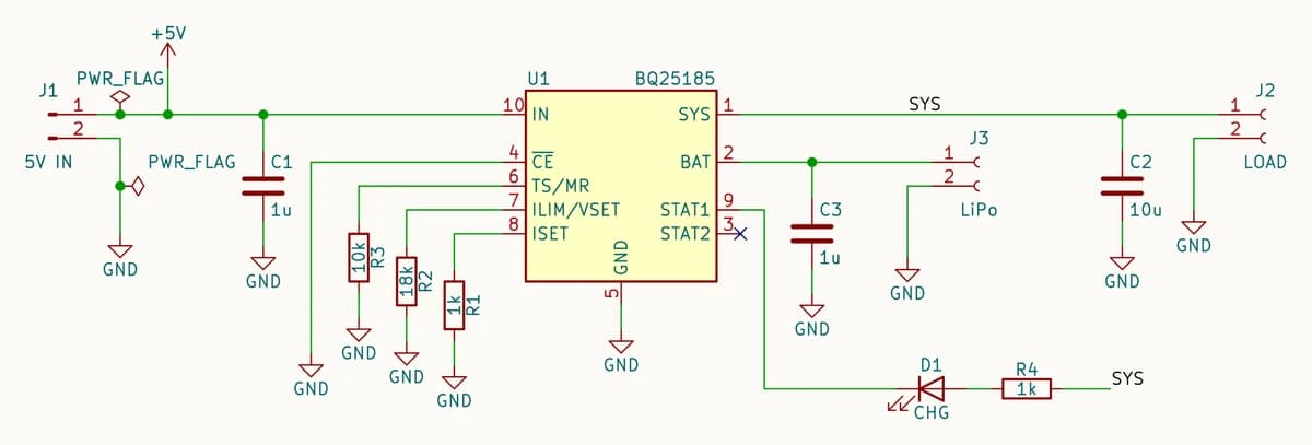
KiCad 9.0.9’s ERC on it: 0 errors and 0 warnings. That needs the two PWR_FLAGs. The 5 V header and the battery connector have passive pins, so without a flag the +5V and GND nets have power inputs and nothing driving them, the classic “Input Power pin not driven” error. SYS and the battery net need no flag, because the BQ25185’s SYS and BAT pins are power outputs. Typing them that way is what makes this work.
Multiple units and symbols from existing ones
A part with several identical sections, like a dual op-amp or a quad NAND gate, is one symbol with several units. Set “Number of units per package:” before adding pins, tick “All units are interchangeable” when the units are identical, and draw each unit with that unit selected. On the schematic they become U1A, U1B and so on. The supply pins can go in a unit of their own: KiCad’s LM358 is two amplifier units and a third with V+ and V−, and its 74LS00 is four gates and a fifth unit with VCC and GND.
To start from an existing symbol, there are two routes. A part that differs only in its name and fields (another voltage or temperature grade) can be a derived symbol: use “Derive from existing symbol:” in the New Symbol dialog, with the base in the same library. A part that needs different pins or graphics is a copy: open the original, File → Save As… into your library under a new name, then edit it. The copy is yours, and KiCad’s library updates will not change it.
If the part is a common one, check KiCad’s library first. KiCad 9 already ships the TP4056, the MCP73831 and the BQ24074, among other chargers; for a whole charger circuit around one, see the ESP32 battery charger circuit.
Common questions
- How do I create a new symbol in KiCad 9?
- Open the Symbol Editor from the project manager or from the Schematic Editor (Tools → Symbol Editor). Select a library you can write to, or make one with File → New Library…. Then File → New Symbol…: give the name, the reference prefix (U, R, J…) and the number of units, and add one pin per pad with the pin number from the datasheet.
- How do I add a symbol to an existing library in KiCad?
- Select that library in the Symbol Editor's library tree before File → New Symbol…; a new symbol goes into the active library. To copy a symbol from another library, open it and use File → Save As… (or Save Copy As…) and pick your library. KiCad's own libraries are usually installed where you can't write; saving into one gives “Library '…' is read-only. Choose a different library to save the symbol '…' to.”
- What electrical type should a GND pin be in KiCad?
- Power input, as KiCad's own library does it. Extra ground pins and an exposed or thermal pad go on the same spot as hidden passive pins, each with its own pad number: stacked, they join the visible pin's net, and being passive they make no hidden connection of their own. Then put a PWR_FLAG on GND, since nothing in KiCad's library outputs ground.
- Why does ERC say “The current configuration does not include the symbol library”?
- The schematic uses a symbol from a library that is in neither your global nor your project symbol library table, for example after copying a sheet from another project. The schematic still has its own copy of the symbol, so it works, but KiCad cannot compare it with the library. Add the library under Preferences → Manage Symbol Libraries…; on the sheet on this page, that took ERC from one warning to none.
- Should I hide power pins in a KiCad symbol?
- No. A hidden pin of type power input is connected to the net with the pin's name, whatever you draw. Name it VSS on a board whose ground is GND and the chip's ground is left on a net of its own. KiCad's manual calls hidden power pins a legacy feature not recommended for new designs, and the symbol checker reports them. Hidden passive pins stacked on a visible pin are fine.
- How do I make a KiCad symbol with multiple units?
- Set the number of units per package in the New Symbol dialog (or later in Symbol Properties) before you add pins, and tick “All units are interchangeable” if the units are identical, like the four gates of a 7400. Draw each unit's pins and graphics with that unit selected; put shared power pins in their own unit or in every unit.
Or describe the charger instead
PCBEditor opens with a LiPo charger described in the chat box. Change it to your own circuit and you get the schematic and the board, with an electrical check before any fab file.
Open the charger in the editor→Sources
ERC reports are copied from kicad-cli’s text output; the date line and sheet header are left out.
- Texas Instruments, BQ25185 datasheet, SLUSF65B (October 2023, revised August 2026): Table 4-1 Pin Functions, Table 6-1 ILIM and VBATREG Resistor Map, the external NTC section (10 kΩ when TS is not used), section 7.2 Typical Application and 7.4 Layout, and the DLH0010A package outline and land pattern (4226298/A).
- KiCad 9.0 Schematic Editor manual (docs.kicad.org): Symbol Editor (creating a library and a symbol, symbol pins, pin electrical types, checking symbols), Managing symbol libraries, and Hidden Power Pins.
- KiCad 9.0.9: the dialog labels and messages quoted, as the program shows them; kicad-cli 9.0.9 sch erc and sch export netlist, run on the sheets on this page.
- KiCad 9.0.9 symbol library: BQ24074RGT, BQ25173DSG, TP4056-42-ESOP8 and MCP73831-2-MC, read for their pin types and stacked pins; LM358 and 74LS00 for their units. Footprint library: Texas_DLH0010A_WSON-10-1EP_2.2x2mm_P0.4mm_EP0.9x1.5mm, read for its pad numbers.