How to verify a PCB with AI: what an automated review catches, and what still needs you
An AI PCB review promises to find the mistakes before the fab does. Some of it delivers: rules and many electrical faults can be checked exactly. Some of it cannot, yet. Here is what a review should check, how PCBEditor’s Review my design does it, a real result on one of our example boards, and the checklist for what is left.
Last reviewed
Short answer
You can verify much of a PCB automatically: design-rule violations, unrouted nets, overlapping parts, shorted connector pins, wrong enable levels and miswired USB connectors are all checked exactly. In PCBEditor, Review my design runs those checks and explains each finding in plain words; the counts come from the checkers, not from a model. What no check catches yet is a circuit that is electrically valid but not what you meant, such as a reset button wired to a spare GPIO. That still needs a datasheet review.
What an AI PCB review should check
A useful review checks the things that can be checked exactly, explains them so you know what to do, and is honest about the rest. Review my design checks four groups and sorts every finding into “must fix” and “worth a look”:
- Design rules
- Clearance between copper, trace width, annular ring, drill-to-drill and hole-to-copper spacing, board-edge margin, unrouted connections, and parts whose courtyards overlap (two parts on one spot cannot both be soldered, so that one counts as must-fix).
- Electrical faults that pass a clean DRC
- The final netlist is audited for mistakes geometry cannot see: connector contacts shorted together, enable pins held at the wrong level, a USB port that back-feeds the supply, a USB connector whose contacts carry the wrong signals, socket rows that do not match the module plugged into them, and nets that reach only one pin.
- Signal and power details
- Pairs such as USB D+ and D- that are not routed side by side, ground areas on different layers that are not stitched together, and a summary of every power path from its source to the parts it feeds.
- Your request
- An AI model compares what you asked for with the parts on the board and names any requested function that has no part, such as a missing regulator or sensor. This is the one judgement in the report, and it is shown separately from the checks.
Each rule or electrical finding comes with a fixed explanation of why it matters and what to do, and the example that triggered it. Those findings and their counts come from the checkers, not from a model. AI does two things: the comparison with your request, and the fixes you ask for.
A real review, step by step
- Open the board. Generate it from a description, draw it, or import a KiCad board, then switch to the PCB view.
- Press Review my design. It runs the checks and changes nothing.
- Read must-fix first.These stop the board from being built or working. “Worth a look” items are judgement calls.
- Fix in plain English.Switch to Build and describe the change, naming the parts and pins (“move C6 away from U3”), or use Fix DRC with AI for rule violations.
- Review again. Every edit can move something else, so run the review after each one.
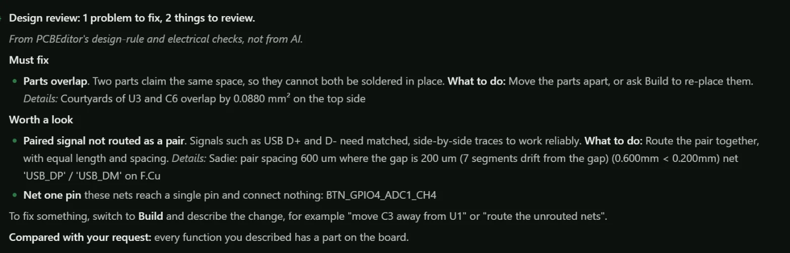
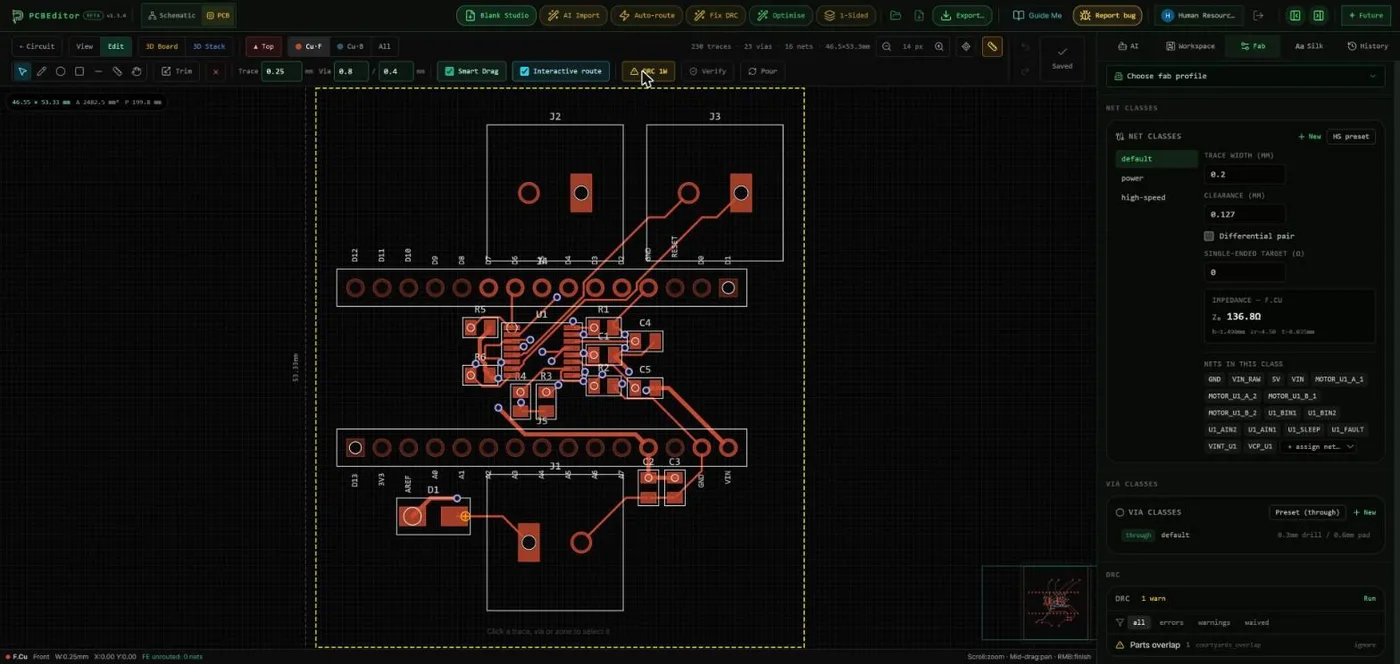
On this board the review found a real problem we had noticed by eye: the regulator U3 and capacitor C6 sit so close that their courtyards overlap, so one of them cannot be placed. It also flagged the USB pair, which was routed 600 µm apart where it should run side by side, and a leftover net from an earlier edit that reaches a single pin.
What it still misses
In our test of six boards generated on 17 October 2026, four passed the design-rule check with a mistake still in them: a reset button wired to a spare GPIO instead of the enable pin, an LED that could never light, a module’s power pin left open, and an I²C clock on a pin without I²C hardware. All four were electrically valid circuits that were not what the prompt asked for. Each was found by reading the datasheets and fixed with one chat edit.
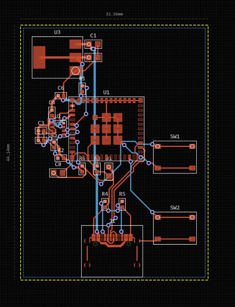
Layout context is the other gap. The module above sat in the middle of the board with its antenna over a ground pour, and the board passed every rule. Checks improve as misses are found, but a final look by someone who knows the parts is still part of verifying a PCB. The full story of all six boards is in AI PCB design, tested on six boards.
Passing every check is not the same as working
Can a chat assistant review a schematic?
A general chat assistant is a good second pair of eyes on a schematic image or a netlist: it will spot a missing pull-up, a capacitor without a ground, or a part used outside its typical circuit, and it explains datasheet details well. It is not a checker. It cannot measure a clearance, it does not trace every pin, and when we asked a model to act as a rule checker on a board summary, it reported different error counts for the same board on different runs. That is why Review my design gets its numbers from the checkers and uses AI only to explain and fix.
A review checklist for the rest
Schematic
- Power: every rail from the connector to each chip, input protection, regulator input range and dropout.
- Ratings: every supply against every part’s absolute maximum, and series parts (diodes, fuses) against the load current.
- Straps: reset, boot and enable pins, each with its pull-up or pull-down and capacitor.
- Special-function pins: I²C, SPI, UART, USB, ADC, crystal and programming header on the pins that have that hardware.
- Required parts: decoupling and bulk capacitors at the datasheet values, not just present.
- Connectors: pinout against the cable or module, including unused contacts such as a USB ID pin.
- Parts list: every part number matches its value and its land pattern.
Layout
- Antennas at the board edge with their keepout clear of copper on every layer.
- Connectors on the edge, facing out, with room for the plug.
- Decoupling capacitors next to the pins they serve; differential pairs routed together.
- Design-rule check against your fab’s rules, then the Gerbers opened in a viewer (the Gerber checklist).
Common questions
- Can AI verify a PCB design?
- Partly. Design rules, unrouted nets, overlapping parts and many electrical faults (shorted connector pins, wrong enable levels, miswired USB connectors) can be checked exactly, and an AI can explain what each finding means and fix it on request. Whether the circuit does what you intended, such as a button on the right pin, still needs a review against the datasheets.
- How do you review an AI-generated PCB layout?
- Run the design-rule and electrical checks first, then read the schematic against the datasheets: power from the connector to every chip, every reset, boot and enable pin, special-function pins such as I2C and USB, supply voltages against part ratings, and required capacitors. Then check the layout for antenna keepouts and connector orientation, and re-check after every edit.
- Can ChatGPT check my schematic?
- A chat assistant can read a schematic image or netlist and point out common mistakes, such as a missing pull-up or decoupling capacitor. It cannot measure clearances or trace every pin; when we asked a model to act as a rule checker on a board summary, it reported different error counts for the same board on different runs. Use it to explain a finding, not to count them.
- Is there a free AI PCB checker?
- PCBEditor's Review my design is free with a free account: it runs the design-rule and electrical checks on the board in the editor and explains each finding, what is wrong, why it matters and what to do. It changes nothing until you ask for a fix.
- What is the difference between a DRC and a design review?
- A design-rule check verifies geometry against manufacturing limits: clearances, widths, drills, edges. A design review also asks whether the circuit is right: connections, pin functions, supply levels and whether the board matches what was asked for. A board can pass DRC and still not work.
- What should a PCB design review checklist include?
- Power paths and ratings, reset, boot and enable straps, special-function pins, required capacitors and their values, connector pinouts, part numbers that match their land patterns, layout keepouts and connector orientation, design-rule check against your fab's rules, and a final look at the Gerbers in a viewer.
Review your own board
Generate or import a board, open it in the editor and press Review my design. A free account is needed for the AI features.
Open the editor→Sources
- PCBEditor Review my design, production build v1.3.4, run on 18 October 2026 on the ESP32-C3 example board.
- PCBEditor six-board test, 17 October 2026: the prompts, exports and pin-by-pin review are on the AI PCB design page.
- IPC-2221B, Generic Standard on Printed Board Design: conductor spacing and sizing.
- IPC-7351B, Generic Requirements for Surface Mount Design and Land Pattern Standard: courtyards.