Your Gerbers passed the upload check. Here’s what it didn’t look at.
You upload a zip, the fab’s page draws a board and shows a price. That proves one thing: their software could read your files. It cannot prove the files describe the board you designed, because the files are all the fab has. A missing outline, holes that land beside their pads or a blank paste layer all quote without complaint.
Last reviewed
Short answer
Before you pay, open the exact zip you are sending in a Gerber viewer and check seven things: the layer count, the board outline, the drill holes, the solder mask, the paste, the silkscreen and the board size. The two mistakes below came straight out of KiCad’s own export, one checkbox each, and both would have priced normally.
What an upload check can and can’t tell you
A fab’s upload step reads each file, works out which layer it is (from the X2 attributes KiCad writes, or from the file name), measures the board, counts holes and layers, and prices the job. Many fabs then review the files after you order and email questions if something looks odd. Both are useful. Neither knows what you meant, so neither can tell you that a layer is missing, that an outline should exist, or that the holes are 100 mm from where they should be.
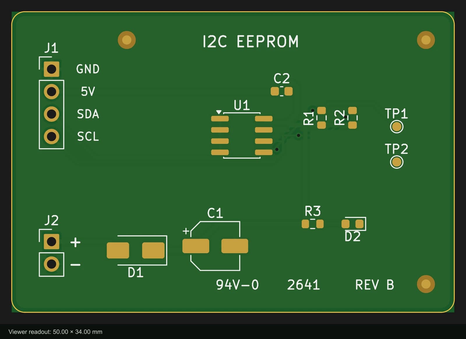
That is the job of a check on your side, on the exact zip you will upload. It takes a few minutes in a Gerber viewer. The rest of this page is what to look at, in the order that catches the expensive mistakes first.
1. Every layer you meant is in the zip
Count the copper layers first: a four-layer board needs four copper files, and a plot dialog with only the outer layers ticked produces a perfectly valid two-layer set. Then check that each side that has solder mask and silkscreen has its own file, that the outline is there, and that there are drill files for plated and, if you have any, non-plated holes.
KiCad also writes a Gerber job file (.gbrjob) listing the layer count, thickness and every file’s function. Some fabs read it. It is a list, not proof: the job file for the board in these pictures lists two paste layers, and both are empty (see check 5).
2. The outline is there, closed, and drawn once
The outline (Edge.Cuts in KiCad, the profile in Gerber terms) is the only file that says where the board ends. Leave it out and every other layer still loads, which is why it is easy to miss. In the viewer below the copper, mask and silkscreen are all present; only the yellow edge is gone.
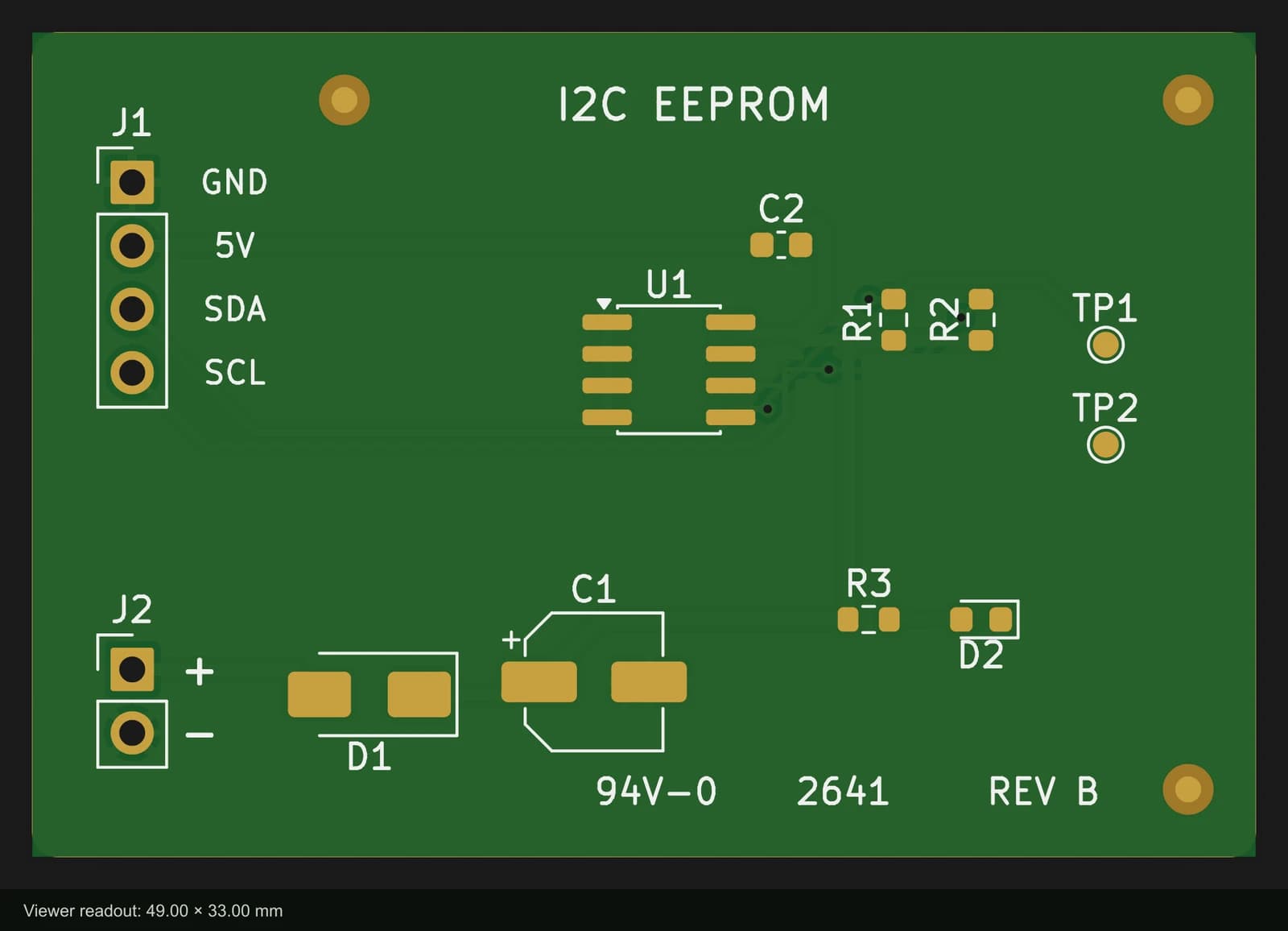
Without it, the board size is a guess. The viewer can only measure the copper, which stops half a millimetre inside the edge, so it reports 49.00 × 33.00 mm for a 50 × 34 mm board. A fab has the same problem and will either guess or ask, and asking costs a day.
An outline can be present and still wrong
3. Every hole lands in its pad
Drill files are a separate format (Excellon) with their own origin and units. If the Gerbers and the drill file were written from different origins, the copper is right and the holes are somewhere else. In KiCad 9’s own dialogs the two origins are one shared setting, so this happens when the files are exported separately: here kicad-cli plotted the Gerbers from the drill/place file origin and wrote the drill file in absolute coordinates, one flag each, as a script, an older KiCad or another tool can:
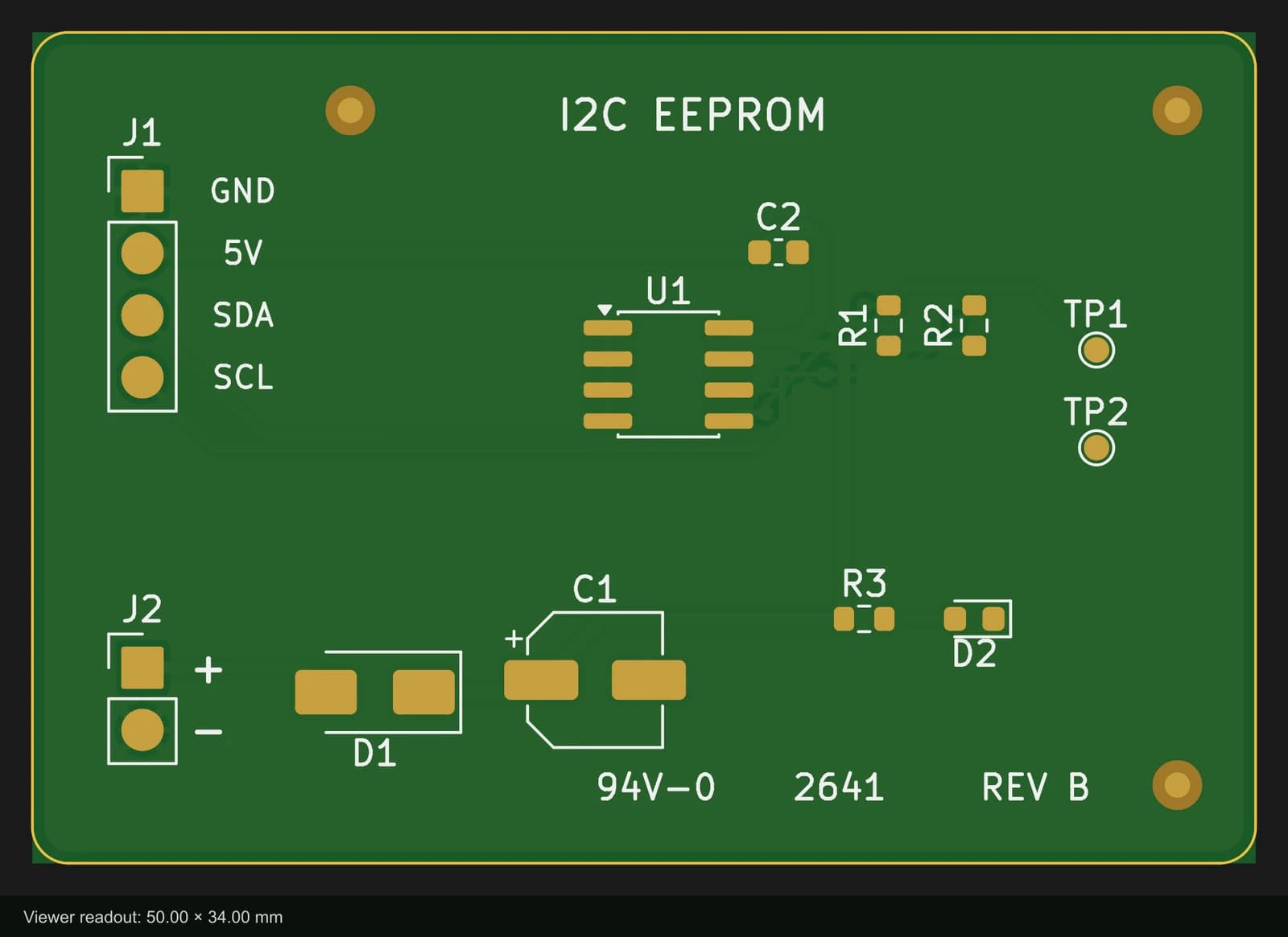
The pads on J1 and J2 are solid gold: the holes are more than 100 mm away, off the board. A smaller origin difference is worse, because the holes land partly in the pads and look almost right. Look at a through-hole part and at a via, and make sure the hole sits in the middle of the copper.
While you are in the drill layer, check that mounting holes are in the non-plated file if they should not be plated, and that the tool sizes in the file match the holes you designed. KiCad writes metric, decimal coordinates by default, which avoids the old zero-suppression ambiguity.
4. The mask opens over every pad, and nowhere else
The solder mask file is a negative: what it draws is where the mask is removed. Turn on one side’s copper and mask together and every pad should show an opening. The vias are the other half of the check. Covered (tented) vias should have no opening; vias you want to probe should.
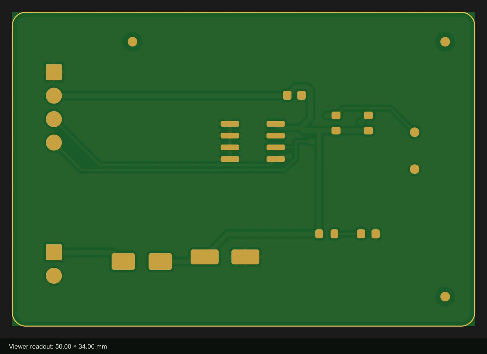
On fine-pitch parts, look at the strip of mask between neighbouring pads. If it is thinner than your fab’s minimum, it is dropped and the pads share one opening, which makes solder bridges more likely.
5. The paste layer isn’t empty
The paste layers matter only if you order a stencil, and then they are the stencil. They should have an opening on every SMD pad and none on through-hole pads. The board in these pictures has 27 SMD pads and empty paste files: we removed the paste to photograph bare copper. Both files are in the zip and both are listed in the job file, so a file count passes. Turn on the paste layers alone and there is nothing to see, and a stencil cut from them would be a blank sheet of steel.
6. The silkscreen stays off the pads
Fabs clip silkscreen that falls on bare copper, so a reference designator printed across a pad comes back cut in half or missing. Check that text is at least your fab’s minimum height and line width, and that the bottom silkscreen reads mirrored when you look at it from the top: that is correct, because you will read it from underneath. For what each marking should say, see how to read the markings on a PCB.
7. The size and stackup match the order form
The viewer’s size readout should match your design, and the order form should match both: board size, layer count, thickness and surface finish. A two-layer zip ordered as four layers, or a 1.6 mm design ordered at 0.8 mm, is a correct set of files and the wrong board.
Then check the design, not just the files
Everything above checks that the files say what the board file says. It does not check the board. Before you export, run your CAD tool’s design-rule check with your fab’s minimum trace, gap, drill and annular ring values, not the defaults. If your fab runs an electrical test, KiCad can also export an IPC-D-356 netlist so the tester knows which pads should connect.
To check that copper connects what you expect, PCBEditor’s viewer has a net tracer: click a trace and it lights every pad, track and via joined to it, across both copper layers.
The checklist
- Open the zip you will upload. Not the folder you exported to, and not the board file. The zip is what the fab gets.
- Count the layers. Copper layers equal to your stackup, mask and silkscreen for each side that has them, the outline, and both drill files.
- Find the outline. Closed, drawn once, cut-outs inside it. The board size in the viewer matches your design.
- Look through every hole. Each through-hole pad has a hole in it, vias sit inside their pads, mounting holes are where the mechanical drawing puts them.
- Read the solder mask. An opening over every pad, none over the vias you meant to cover, and no slivers between fine-pitch pads thinner than your fab can make.
- Check the paste, if you are ordering a stencil. Openings on SMD pads only, and not an empty file.
- Read the silkscreen. Nothing printed on pads, text large enough for the fab's minimum, the bottom side reading mirrored when seen from the top.
- Match the order form. Size, layer count, thickness and finish on the form agree with the files.
Common questions
- How do I check Gerber files before ordering?
- Open the zip you will upload in a Gerber viewer and check the layer count, the board outline, that every hole sits in its pad, the solder mask openings, the paste layer if you order a stencil, the silkscreen and the board size. Then compare the size, layer count and thickness with the order form.
- Why are my drill holes offset from the pads?
- The Gerbers and the drill file were written from different origins. In KiCad 9's own dialogs "Use drill/place file origin" (Plot) and the drill origin (Generate Drill Files) are one shared setting, so the mismatch usually comes from files exported separately: from kicad-cli, an older KiCad version or another tool. Export both from the same place with the same origin.
- What happens if the board outline layer is missing?
- There is no board edge in the files, so the fab has to guess the size from the copper or ask you. In KiCad, tick Edge.Cuts in the plot dialog and export again.
- Does the fab check my Gerber files?
- Its software reads them to identify the layers, measure the board and price it, and many fabs review the files after you order and email questions. Neither compares the files with what you intended, because the files are all the fab has.
- Which files does a two-layer PCB need?
- Top and bottom copper, top and bottom solder mask, top and bottom silkscreen, the board outline, and the drill files (plated and non-plated). Paste layers are needed only if you order a stencil.
Open your zip before you pay
PCBEditor’s Gerber viewer reads the zip in your browser, with no sign-up: every layer, the drills, the outline and the board size, plus a net tracer that follows a trace from pad to pad.
Open the Gerber viewer→Sources
Every image is PCBEditor’s Gerber viewer opening files that kicad-cli 9.0 exported from one board. The broken sets come from export settings, not hand edits.
- Ucamco, The Gerber Layer Format Specification (RS-274X with X2 attributes): file functions, regions and the profile (outline) layer.
- IPC-NC-349 / Excellon format: tool table, units and coordinate format in drill files.
- KiCad 9 documentation: Fabrication outputs (Plot, Generate Drill Files, Gerber job file, IPC-D-356 netlist).