Schematic to PCB: from a KiCad schematic to a board, with nothing lost
Turning a schematic into a PCB moves three things onto the board: a footprint for every symbol, a net on every pad, and the link between them, made by matching pin numbers to pad numbers. The failures are mostly quiet. A pin whose number has no pad never gets connected, and nothing later in the flow will notice. Here is the KiCad 9 procedure, every message it can stop on, and a check that proves the board matches the schematic, run on a real USB-C sensor board.
Last reviewed
Short answer
In KiCad 9, open the project from the KiCad project manager, annotate, assign a footprint to every symbol and run ERC, then use Tools → Update PCB from Schematic… (F8) in either editor. Read the report before you press Update PCB: a line like “J1 pad S1 not found” means a connection that will not exist on the board. Before you order, run DRC with “Test for parity between PCB and schematic”. To turn a schematic into a placed and routed board automatically, import the .kicad_sch into an AI PCB tool, then check the result the same way.
What moves from the schematic to the board
Three things, and only three. Each symbol brings the footprint named in its Footprint field. Each pad takes the net of the symbol pin with the same number: KiCad’s documentation puts it in one line, “symbol pins are matched to footprint pads by pin/pad number.” And the reference ties the two together, so later updates find the same footprint again.
Nothing else moves. The footprints arrive with ratsnest lines between pads of the same net; board outline, placement and routing come after. That is why the update itself rarely fails loudly: it only has to copy, and the mistakes it can make are copying something incomplete.
In KiCad 9: Update PCB from Schematic
- Open the project (.kicad_pro) from the KiCad project manager, and open the schematic and the board from there.
- Tools → Annotate Schematic…, so every symbol has a unique reference.
- Tools → Assign Footprints… until every symbol that goes on the board has a footprint.
- Run ERC and fix what it finds: the board can only be as connected as the schematic.
- Tools → Update PCB from Schematic… (F8), from either editor. Read the report, then press Update PCB.
The dialog has six options. Their labels are KiCad’s; the descriptions follow KiCad’s documentation.
| Option | What it does |
|---|---|
| Re-link footprints to schematic symbols based on their reference designators. | Rebuilds the link between each footprint and its symbol from the reference. KiCad’s documentation says it should generally be left unchecked. |
| Replace footprints with those specified by symbols. | Swaps a footprint on the board when you changed the symbol’s footprint. Unchecked, footprints already on the board are not changed. |
| Delete footprints with no symbols. | Removes footprints that have no symbol in the schematic. Read the report first: it lists every footprint it will remove. |
| Override locks. | Unchecked, locked footprints are never deleted or replaced, even when they otherwise would be. |
| Update footprint fields from symbols. | Copies field values (value, MPN and the like) from each symbol to its footprint. |
| Remove footprint fields not found in symbols. | Deletes fields on a footprint that its symbol no longer has. |
The first time, leave them as they are. Later, after you change a part’s footprint in the schematic, tick “Replace footprints with those specified by symbols”, or the board keeps the old one.
When it won’t update: the messages and their fixes
These are KiCad 9’s own messages, word for word; ‹ › marks the parts that change. Most are in the report that Update PCB from Schematic shows before it changes anything.
| KiCad says | Why | Fix |
|---|---|---|
| Cannot update the PCB because PCB editor is opened in stand-alone mode. In order to create or update PCBs from schematics, you must launch the KiCad project manager and create a project. | The board or the schematic was opened on its own, not from a project. | Open the .kicad_pro in the KiCad project manager (or create a project and put both files in its folder), then open both editors from there. |
| Cannot add R1 (no footprint assigned). | The symbol has no footprint, so there is nothing to put on the board. | Tools → Assign Footprints… in the Schematic Editor, then update again. |
| Cannot add J1 (footprint '…' not found). | The footprint’s library nickname is not in your footprint library table, or the name is misspelled. | Add the library under Manage Footprint Libraries…, or pick the footprint again from a library you have. |
| ‹ref› pad ‹number› not found in ‹footprint›. | The symbol has a pin whose number no pad on the footprint carries. That pin’s connection is not made on the board. | Use a footprint whose pad numbers match the symbol’s pin numbers, or renumber one of them. See the shield section below. |
| No net found for component ‹ref› pad ‹pad› (no pin ‹pin› in symbol). | The footprint has a numbered pad that no symbol pin matches, so it gets no net. | Fine for a pad that should float. If it is a shell or a thermal pad, give the symbol that pin or the pad the right number. |
| Schematic parity tests require a fully annotated schematic. | Some references are still R?, C? and so on. | Tools → Annotate Schematic… before you update or run DRC. |
The one that costs a respin
The quiet failure: shield and shell pins
Connector shells are where pin and pad numbers drift apart most often, because every library numbers them its own way. In KiCad 9’s own libraries, the footprint and the symbol agree, and the number changes with the connector family:
| Connector | Footprint (example) | Symbol, shield pin | Shell pad number |
|---|---|---|---|
| USB-C receptacle | USB_C_Receptacle_HRO_TYPE-C-31-M-12 | USB_C_Receptacle_USB2.0_16P, pin S1 “SHIELD” | S1 |
| Micro-USB | USB_Micro-B_Amphenol_10104110_Horizontal | USB_B_Micro, pin 6 “Shield” | 6 |
| USB-A | USB_A_CNCTech_1001-011-01101_Horizontal | USB_A, pin 5 “Shield” | 5 |
| D-sub 9 | DSUB-9_Socket_Horizontal_…_Housed_… | DE9_Socket_MountingHoles, pin 0 “PAD” | 0 |
Mix a symbol from one source with a footprint from another, one that calls the shell “SH”, “MP” or “SHIELD”, and the shield pin has no pad. The shell lugs are still soldered to the board, just to nothing. On a USB-C board that usually means the shield is not tied to ground, which shows up later as ESD and emissions trouble rather than as a dead board.
Two kinds of pad are meant to have no net: pads with no number at all (the plastic locating pegs on the USB-C and USB-A footprints above are unnumbered) and pins you mark as not connected. Anything else without a net deserves a look.
Prove the board matches the schematic
KiCad has a built-in comparison: in the PCB Editor’s DRC, tick “Test for parity between PCB and schematic”. It reports missing footprints, values that differ from the symbol, pins with no pad, pads with no pin, and pads whose net differs from the schematic. From the command line it is kicad-cli pcb drc --schematic-parity --severity-all --exit-code-violations, which fails the run when anything differs. KiCad AI shows a real run that caught one changed resistor value.
We ran it on a board whose USB-C footprint numbered its shell “SH”. kicad-cli’s report found 0 DRC violations and 0 unconnected pads, and among the parity results, exactly the missing connection:
[net_conflict]: No pad found for pin S1 (GND) in schematic.
    Local override; warning
    @(18.7000 mm, 23.5000 mm): Footprint J1
The parity test compares net names as well as connections. A board that went through another tool can therefore show net_conflict lines for nets that are wired right but named differently (“SCL” for KiCad’s “/SCL”), and for unused pins whose pads have no net where KiCad expects an “unconnected-(…)” one. Read the message: “No pad found for pin” is a missing connection; “Pad net (A) doesn’t match net given by schematic (B)” may only be a name.
To separate naming from wiring, take KiCad’s own netlist (kicad-cli sch export netlist) and compare which pads share a net on the board. These are the nets of the board below, as the netlist names them; on the exported board every one has exactly these pads:
| Net | Pads (kicad-cli netlist; the same on the board) |
|---|---|
| GND | C1.2 C2.2 C3.2 C4.2 J1.A1 J1.A12 J1.B1 J1.B12 J1.S1 J2.2 R1.2 R2.2 U1.2 U2.1 U2.5 U2.7 |
| VBUS | C1.1 J1.A4 J1.A9 J1.B4 J1.B9 U1.1 U1.3 |
| +3V3 | C2.1 C3.1 C4.1 J2.1 R3.1 R4.1 U1.5 U2.2 U2.6 U2.8 |
| /SCL | J2.3 R3.2 U2.4 |
| /SDA | J2.4 R4.2 U2.3 |
| Net-(J1-CC1) | J1.A5 R1.1 |
| Net-(J1-CC2) | J1.B5 R2.1 |
| unconnected-(…), one per pin | J1.A6 J1.A7 J1.A8 J1.B6 J1.B7 J1.B8 U1.4 |
The row worth checking first is GND: J1.S1 is there, and on the board all four of J1’s shell lugs carry it. The last row is just as important the other way round: the USB data and sideband pins and the regulator’s NC pin are unused in this design, and they must stay without a net.
Schematic to PCB with AI
The step KiCad leaves to you, placing and routing, is the one an AI PCB tool takes over. In PCBEditor you drop every .kicad_sch of a KiCad 6 to 9 project (sub-sheets included, or the zipped project) into Workspace > KiCad Native. The schematic opens with KiCad’s connections and your footprints, and Approve → Generate PCB builds the board from it.
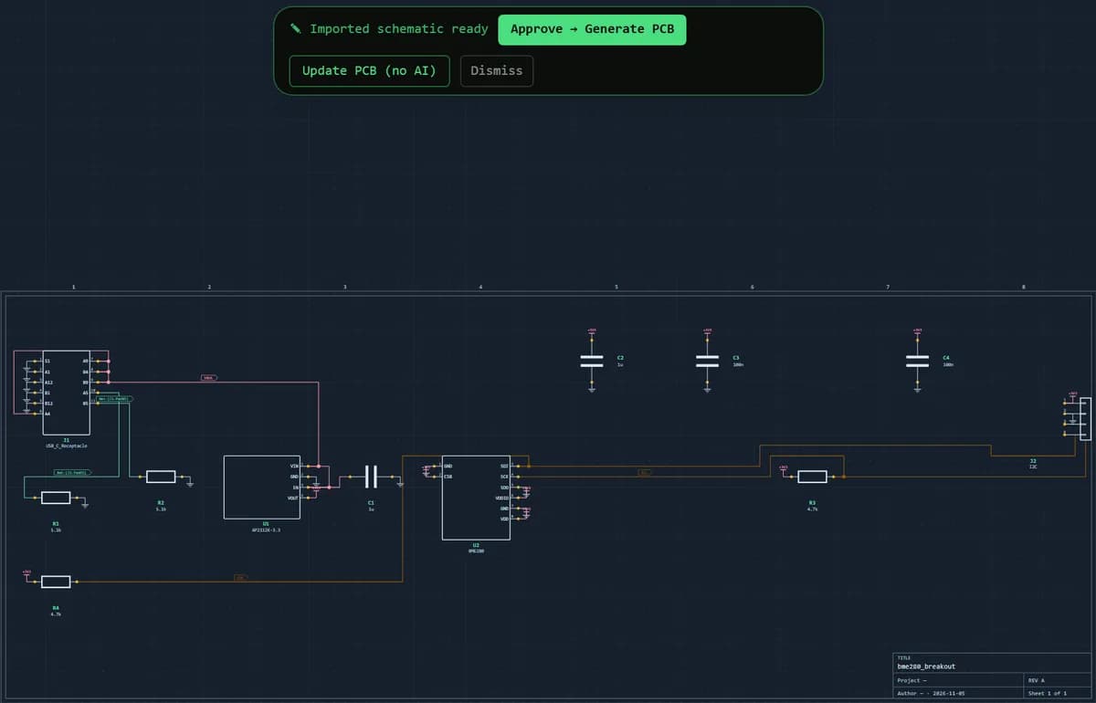
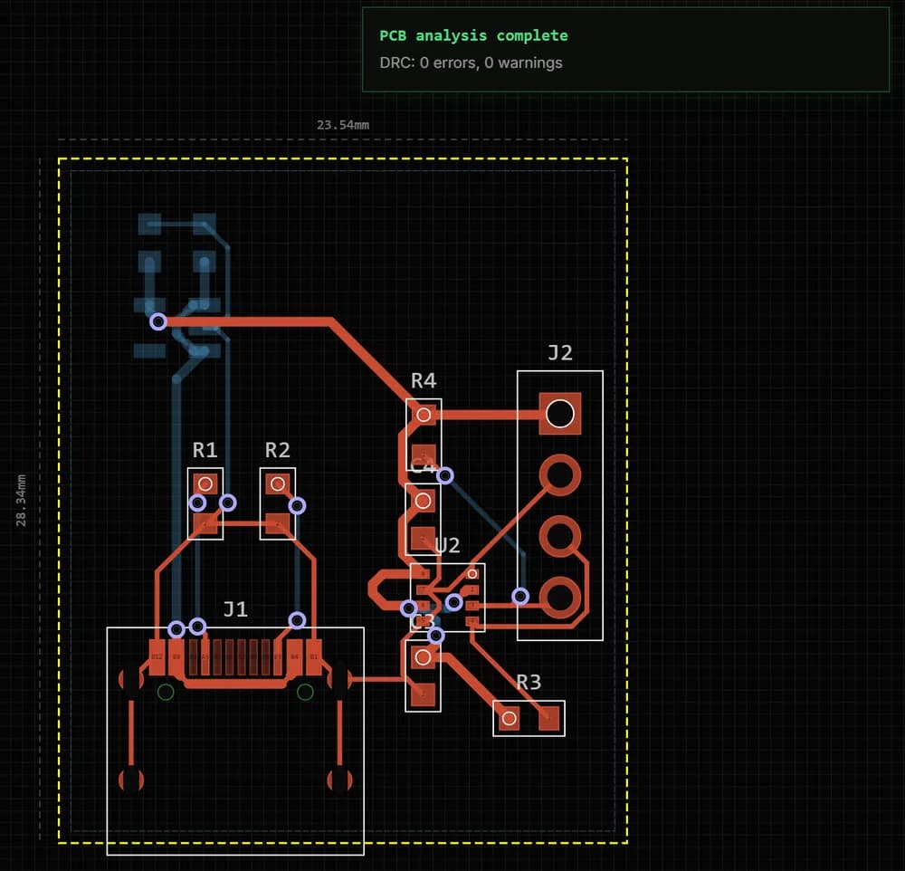
The schematic here is a USB-C powered BME280 breakout drawn in KiCad 9: 12 parts, an AP2112K-3.3, 5.1 kΩ on each CC pin, 4.7 kΩ I²C pull-ups and a four-pin header. The generated board is two layers, 23.54 × 28.34 mm, with every net routed and DRC at 0 errors and 0 warnings. Exported back as a KiCad board, every net has exactly the pads the kicad-cli netlist in the table above gives it, shield included. Two auto-named nets carry different names (Net-(J1-PadA5) for Net-(J1-CC1)), which is why the comparison is by pads, not by name.
Then review it like a colleague’s first pass. On this board the regulator and its two capacitors went on the bottom side, which means a second assembly pass; if you want everything on top, say so and generate again. Also check that connectors sit on the edge you want and that the sensor is away from the regulator’s heat. A matching netlist proves the board is connected as drawn, not that it is placed as you would.
Common questions
- How do I convert a schematic to a PCB in KiCad?
- Open the project from the KiCad project manager, annotate the schematic, assign a footprint to every symbol and run ERC. Then choose Tools → Update PCB from Schematic… (F8) in the Schematic Editor or the PCB Editor, read the report and press Update PCB. The footprints arrive with their nets as ratsnest lines; placement and routing are still yours to do.
- Why won’t KiCad update the PCB from the schematic?
- The most common reason is stand-alone mode. KiCad then says: “Cannot update the PCB because PCB editor is opened in stand-alone mode. In order to create or update PCBs from schematics, you must launch the KiCad project manager and create a project.” Open the .kicad_pro from the project manager and both editors from there. If it updates but parts are missing, look for “Cannot add … (no footprint assigned)” in the report.
- Do schematic pin numbers have to match footprint pad numbers?
- Yes. KiCad’s documentation says it plainly: symbol pins are matched to footprint pads by pin/pad number. A pin numbered S1 needs a pad numbered S1. Names do not count, only numbers.
- Why is my USB-C shield not connected on the PCB?
- Usually because the footprint numbers the shell pads differently from the symbol’s shield pin. In KiCad’s own libraries both use S1 for USB-C receptacles. A footprint from elsewhere that calls the shell “SH” or “MP” leaves the pin with no pad, and Update PCB reports “J1 pad S1 not found”. Match the numbers and update again.
- How do I check that my PCB matches the schematic?
- Run DRC with “Test for parity between PCB and schematic” checked, or kicad-cli pcb drc --schematic-parity from the command line. For a pad-by-pad proof, export KiCad’s netlist with kicad-cli sch export netlist and compare every pad’s net on the board with it.
- Is there an AI that converts a schematic to a PCB?
- Yes. PCBEditor imports KiCad 6 to 9 schematics (every .kicad_sch, sub-sheets included, or a zipped project) and places and routes the board from KiCad’s own connections. Export the result as a KiCad project and check it against the netlist like any other board.
Turn your KiCad schematic into a routed board
Open the editor, go to Workspace > KiCad Native and drop your .kicad_sch files. It keeps your footprints and KiCad’s connections, places and routes the board, and exports it back as a KiCad project.
Import a KiCad schematic→Sources
The board on this page was generated on 5 November 2026 from a KiCad 9 schematic drawn for it; the netlist and the exported board are compared pad by pad, not by count.
- KiCad 9.0 documentation, PCB Editor: “Starting from a schematic” (Tools → Update PCB from Schematic…, F8) and “Adding footprints to the board” (“Symbol pins are matched to footprint pads by pin/pad number.”).
- KiCad 9.0 documentation, Schematic Editor: “Update PCB from Schematic (forward annotation)” and its six options.
- KiCad 9.0 message and menu text, read from the official kicad/kicad:9.0 image: the stand-alone refusal, “Cannot add … (no footprint assigned)”, “Cannot add … (footprint … not found)”, “… pad … not found in …”, “No net found for component … pad … (no pin … in symbol)”, “Schematic parity tests require a fully annotated schematic”, “Test for parity between PCB and schematic”.
- KiCad 9 footprint and symbol libraries: shell pads S1 (USB-C), 6 (micro-USB), 5 (USB-A) and 0 (D-sub), with the same numbers on the matching symbols’ shield pins.
- kicad-cli 9.0.9: sch export netlist, used as the reference for the pad-by-pad comparison.