How wide does a PCB trace need to be for 1 A, 2 A, 3 A or 5 A?
The usual answer is a table, and most tables are the same IPC-2221 formula at different settings. That is a fine starting point for an outer-layer trace on an ordinary board. It is too generous for some boards, far too cautious for internal layers, and it says nothing about voltage drop, which is often the limit that bites first.
Last reviewed
Short answer
On 1 oz copper on an outer layer, allowing a 10 °C rise: about 0.30 mm (12 mil) for 1 A, 0.78 mm (31 mil) for 2 A, 1.37 mm (54 mil) for 3 A and 2.77 mm (109 mil) for 5 A. Allow 20 °C and they shrink by about a third; use 2 oz copper and they halve. Then check the voltage drop: at 1 A, 100 mm of that 0.30 mm trace drops 175 mV.
The table
Width for a continuous current, from the IPC-2221 formula. The first three columns are outer layers (top or bottom), the last is an internal layer.
| Current | 1 oz outer, 10 °C | 1 oz outer, 20 °C | 2 oz outer, 10 °C | 1 oz internal, 10 °C |
|---|---|---|---|---|
| 0.5 A | 0.12 mm (5 mil) | 0.08 mm (3 mil) | 0.06 mm (2 mil) | 0.30 mm (12 mil) |
| 1 A | 0.30 mm (12 mil) | 0.20 mm (8 mil) | 0.15 mm (6 mil) | 0.78 mm (31 mil) |
| 2 A | 0.78 mm (31 mil) | 0.51 mm (20 mil) | 0.39 mm (15 mil) | 2.03 mm (80 mil) |
| 3 A | 1.37 mm (54 mil) | 0.90 mm (35 mil) | 0.68 mm (27 mil) | 3.56 mm (140 mil) |
| 5 A | 2.77 mm (109 mil) | 1.82 mm (71 mil) | 1.38 mm (54 mil) | 7.19 mm (283 mil) |
| 10 A | 7.19 mm (283 mil) | 4.72 mm (186 mil) | 3.60 mm (142 mil) | 18.71 mm (737 mil) |
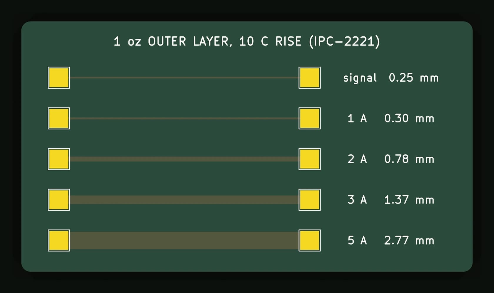
The coupon makes the jump visible: going from 1 A to 5 A takes the trace from barely wider than a signal trace to over 2.7 mm. At 10 A the 1 oz outer width passes 7 mm, which is the point to stop widening traces and use a copper pour, heavier copper or both.
How to read it: rise, copper weight, layer
Temperature rise is how much hotter than its surroundings the trace may run. It is a choice, not a property of the board. 10 °C is the cautious default; 20 °C shrinks every width by about a third.
Copper weight is thickness: 1 oz is about 35 µm, 2 oz is twice that. Current capacity follows cross-section, so 2 oz copper roughly halves the width. Check what your fab charges for it; on budget fabs the outer layers are 1 oz unless you ask.
Layer is where IPC-2221 is most conservative. Its formula halves the constant for internal layers, which makes an internal trace about 2.6 times as wide as an outer one for the same current.
What IPC-2152 changed
IPC-2221’s external chart comes from US National Bureau of Standards tests in the 1950s, and its internal chart was never tested: it was derived from the external one. IPC-2152, published in 2009, replaced both with new measurements, and two findings matter for everyday boards. First, internal traces are not the poor relations IPC-2221 makes them: in the new tests internal and external traces carrying the same current ran at close to the same temperature rise, internal ones slightly cooler, so the 2.6× internal penalty is mostly margin. Second, the trace is only part of the story. Board thickness and copper planes near the trace change the temperature rise as much as the width does, which is why IPC-2152 gives a baseline chart (3 oz copper, still air, no planes) plus modifiers for copper weight, planes, board thickness and environment.
In practice: the IPC-2221 table is a safe outer-layer answer for a board in open air. If a trace runs over or beside a solid plane, it runs cooler than the table says. If the board sits in a sealed box, it runs hotter.
Wide enough for heat is not wide enough for voltage
The width tables size a trace so it does not get too hot. They do not look at how much voltage it loses on the way. Here is 100 mm of each heat-sized trace from the first column, with the copper at 35 °C:
| Current | Width | Resistance | Voltage drop | Heat in the trace |
|---|---|---|---|---|
| 1 A | 0.30 mm | 175 mΩ | 175 mV | 175 mW |
| 2 A | 0.78 mm | 67 mΩ | 135 mV | 269 mW |
| 3 A | 1.37 mm | 38 mΩ | 115 mV | 345 mW |
| 5 A | 2.77 mm | 19 mΩ | 95 mV | 473 mW |
175 mV is about 5% of a 3.3 V rail, gone before the current reaches the load. For a supply that feeds a regulator that may not matter; for the rail a microcontroller or sensor runs from, it often does. Work out the drop for your length with the trace resistance calculator, and widen the trace, or bring the load closer, until it is small enough.
Return current needs the same width
When the table is wrong
- Short necks are fine. Thermal modelling by Brooks and Adam shows a trace that narrows for a few millimetres to enter a pad runs cooler than a long trace of that width, because the wide copper on each side draws heat away. The benefit shrinks as the neck gets longer; the table is for long runs.
- Pulsed and switching currents heat a trace by their RMS value, not their peak. A motor that draws 5 A at start-up for half a second does not need a 5 A continuous trace, but a regulator’s switching loop at high frequency needs a short, wide path for reasons that have nothing to do with heat.
- Vias are the bottleneck. A power path that changes layer through one small via is limited by that via, not the trace. Use several, and size them with the via current calculator.
- Enclosures and hot neighbours raise the starting temperature. A 10 °C rise on a board that already sits at 60 °C beside a regulator is a 70 °C trace.
- Above about 10 A on 1 oz copper, the widths stop being practical traces. Use a pour, heavier copper on the power layers, or a bus bar.
How PCBEditor sizes power traces
When your description states a current, say “the motor rail carries 3 A”, PCBEditor sizes that power net with the same IPC-2221 formula at a 10 °C rise for the copper weight of the board, and routes it at that width. If a net would need more than 6 mm, it lays 6 mm and tells you to use a copper pour, 2 oz copper or a bus bar for that path, and any power trace that ends up narrower than its current needs is reported from the copper actually laid. Without a stated current, power nets are routed up to 1 mm wide, narrowed only where the pins they connect to are narrower.
Common questions
- How wide should a PCB trace be for 1 amp?
- On an outer layer of 1 oz copper with a 10 °C rise, about 0.30 mm (12 mil) by IPC-2221. A common rule of thumb is 0.5 mm (20 mil) for 1 A, which also keeps the voltage drop down on longer runs.
- How wide should a trace be for 3 amps?
- About 1.37 mm on 1 oz outer copper with a 10 °C rise, or 0.68 mm on 2 oz. On an internal layer IPC-2221 asks for 3.6 mm, which IPC-2152 shows is very cautious.
- What is the difference between IPC-2221 and IPC-2152?
- IPC-2221's external chart comes from US National Bureau of Standards tests in the 1950s, and its internal chart was derived from it rather than tested. IPC-2152 (2009) is based on new measurements: internal and external traces run at close to the same temperature rise, and board thickness and nearby copper planes change the rise as much as the width does.
- Does a trace need to be as wide as the table along its whole length?
- The table is for long runs. Thermal modelling by Brooks and Adam shows a short narrow section, such as a trace necking down into a pad, runs cooler than a long trace of the same width, because the wider copper on each side draws heat away. The benefit shrinks as the neck gets longer.
- Is a 10 °C or 20 °C temperature rise better?
- 10 °C is a conservative default. 20 °C is common for power traces on boards with thermal margin. Either way, add the rise to the hottest ambient the board will see and keep the total well inside what the board material and parts are rated for.
Work out your own trace, then let the router keep it
The calculator gives the width for your current, copper and temperature rise. In PCBEditor, state the current in your description and the power net is routed at that width.
Open the trace width calculator→Sources
The tables are computed by the same code as PCBEditor’s trace width and trace resistance calculators, so the numbers here and in the tools match.
- IPC-2221B, Generic Standard on Printed Board Design, section 6.2: conductor sizing formula I = k·ΔT^0.44·A^0.725, k = 0.048 external, 0.024 internal.
- IPC-2152, Standard for Determining Current Carrying Capacity in Printed Board Design (2009).
- Copper resistivity 1.724 × 10⁻⁸ Ω·m at 20 °C, temperature coefficient 0.00393 /°C. The calculators take 1 oz copper as 34.8 µm (1.37 mil); IPC-4562A's nominal is 34.3 µm.
- Douglas Brooks and Johannes Adam, thermal modelling of necked-down traces (PCD&F, 2018).