KiCad “Text thickness out of range”: why 0.15 mm becomes 0.125 mm, and how to fix every label at once
You type 0.15 mm for a reference’s line width, set the design rule to 0.15 mm, and KiCad still warns that the text thickness is out of range with “actual 0.125 mm”. That exact report reached the KiCad forum this week. The number is not a bug: KiCad caps the line width at a quarter of the text size. This page reproduces the warning on a KiCad 9 board and covers the text size you need for a given line width, what fabs ask for, why bold makes small text thinner, and how to resize every label in one go.
Last reviewed
Short answer
KiCad draws a text line no wider than a quarter of the text’s smaller dimension, whatever you typed. A 0.5 mm reference with a 0.15 mm line is drawn 0.125 mm wide, and DRC checks the drawn width. For a minimum line width T, make the text at least 4 × T tall and wide: 0.6 mm for 0.15 mm. Fabs ask for more anyway: JLCPCB wants text at least 1.0 mm tall and PCBWay 0.8 mm, both with 0.15 mm lines. Fix all references at once with Edit → Edit Text & Graphics Properties, or lower the rule only if your fab allows it.
Why “actual 0.125 mm” when you typed 0.15
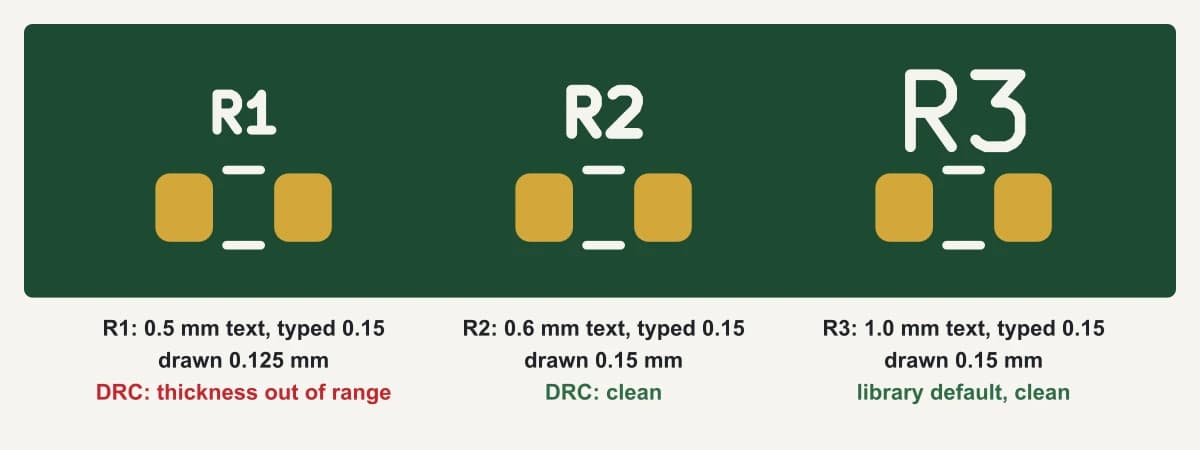
The forum report: references 0.5 mm wide and 0.5 mm tall, line width 0.15 mm, a design rule warning below 0.15 mm, and a warning anyway. At 0.6 mm the warning went away. The test board below reproduces it on KiCad 9.0.9 with three library 0603 resistors whose references are 0.5, 0.6 and 1.0 mm tall, all typed with a 0.15 mm line, and the Board Setup minimums set to 0.5 mm height and 0.15 mm thickness:
[text_thickness]: Text thickness out of range (board setup constraints silk text thickness min thickness 0.1500 mm; actual 0.1250 mm)
    Rule: board setup constraints silk text thickness; warning
    @(103.0000 mm, 103.7000 mm): Reference field of R1
Only R1 fails. KiCad keeps your 0.15 mm in the file but draws the strokes at most a quarter of the text’s smaller dimension, and the design rules check reads the drawn width. Measured on the same board for several sizes:
| Text size | Line width typed | Line width drawn |
|---|---|---|
| 0.5 × 0.5 mm | 0.15 mm | 0.125 mm |
| 0.5 wide × 0.8 tall | 0.15 mm | 0.125 mm |
| 0.8 wide × 0.5 tall | 0.15 mm | 0.125 mm |
| 0.6 × 0.6 mm | 0.15 mm | 0.15 mm |
| 1.0 × 1.0 mm | 0.25 mm | 0.25 mm |
| 1.0 × 1.0 mm | 0.30 mm | 0.25 mm |
Width counts as much as height: narrow text with full height is capped the same way. The rule of thumb that follows is simple. For a minimum line width T, the text must be at least 4 × T in both directions: 0.6 mm for 0.15 mm, 0.48 mm for 0.12 mm. KiCad’s text dialog has a warning for the same thing, “Text thickness is too large for the text size.”
Lowering the rule hides the warning, not the problem
“Text height out of range” and the KiCad defaults
The minimums live in Board Setup → Design Rules → Constraints, as “Minimum text height” and “Minimum text thickness”. On a new KiCad 9 board they are 0.8 mm and 0.08 mm. With those defaults, the 0.5 and 0.6 mm references fail on height instead:
[text_height]: Text height out of range (board setup constraints silk text height min height 0.8000 mm; actual 0.5000 mm)
    Rule: board setup constraints silk text height; warning
    @(103.0000 mm, 103.7000 mm): Reference field of R1
[text_height]: Text height out of range (board setup constraints silk text height min height 0.8000 mm; actual 0.6000 mm)
    Rule: board setup constraints silk text height; warning
    @(108.0000 mm, 103.7000 mm): Reference field of R2
Both checks apply to silkscreen text only. The same 0.5 mm text with a 0.05 mm line on a copper layer and on the fabrication layer produced no warning; on the silkscreen it produced both. Both are warnings by default: kicad-cli pcb drc lists them unless you pass --severity-error, and a check that only counts errors lets the board through.
For reference, new silkscreen text in KiCad 9 defaults to 1.0 mm with a 0.1 mm line, and the library’s 0603 resistor carries its reference at 1.0 mm with a 0.15 mm line. The fabrication layer copy of the reference is 0.4 mm with a 0.06 mm line, which is fine because nothing prints it.
What text size your fab can print
A design rule should be your fab’s number, not a guess. Two common fabs publish theirs:
| Source | Line width | Text height | Notes |
|---|---|---|---|
| KiCad 9, new board | 0.08 mm (minimum) | 0.8 mm (minimum) | Text defaults: 1.0 mm, 0.1 mm line |
| KiCad 9 library footprints | 0.15 mm | 1.0 mm | Reference on the silkscreen |
| JLCPCB | 0.15 mm | 1.0 mm (40 mil) | Line to height 1:6; pad to silkscreen 0.15 mm |
| PCBWay | 0.15 mm | 0.8 mm | Line to height 1:5 |
The 0.15 mm line in the forum report matches both fabs. At either fab, the 0.5 mm text is also below the minimum height, which KiCad would only report if the height minimum were set to match. A library reference, 1.0 mm with a 0.15 mm line, meets both. A reply in the same thread reports 0.64 mm tall text with 0.13 mm lines coming out readable from three US fabs, though the poster needs a loupe to read it. Smaller is possible, but it is the fab’s promise that matters, so set both minimums from its capabilities page and let DRC hold you to them.
Bold makes small text thinner
Ticking Bold replaces your line width with one fifth of the text size. Above 0.75 mm that is thicker than 0.15 mm; below it, thinner. A 0.6 mm reference passes at 0.15 mm, but in bold it is drawn 0.12 mm wide:
[text_thickness]: Text thickness out of range (board setup constraints silk text thickness min thickness 0.1500 mm; actual 0.1200 mm)
    Rule: board setup constraints silk text thickness; warning
    @(108.0000 mm, 103.7000 mm): Reference field of R2
Bold 0.5 mm text gets a 0.1 mm line. If you want heavier small labels, make them larger rather than bold.
Change all text at once
Edit → Edit Text & Graphics Properties opens a dialog that edits many items in one pass. Tick Reference designators, plus any other footprint fields that print, enter the new size and line width, or use “Set to layer default values” to apply the defaults from Board Setup, then apply. Filters narrow it by layer, net, net class or reference designator, which helps when only the tiny parts need changing.
Outside the editor, the same fix is a few lines of pcbnew Python. This script raises every visible silkscreen field below the smallest size that passes the board’s own minimums, and leaves larger text alone:
import sys, pcbnew
b = pcbnew.LoadBoard(sys.argv[1])
ds = b.GetDesignSettings()
# KiCad draws a line at most 1/4 of the text size, so the smallest size that passes is
# the larger of the minimum height and 4 x the minimum thickness.
low = max(ds.m_MinSilkTextHeight, 4 * ds.m_MinSilkTextThickness)
for fp in b.GetFootprints():
    for f in fp.GetFields():
        if f.IsVisible() and f.GetLayer() in (pcbnew.F_SilkS, pcbnew.B_SilkS):
            s = f.GetTextSize()
            if min(s.x, s.y) < low:
                f.SetTextSize(pcbnew.VECTOR2I(max(s.x, low), max(s.y, low)))
pcbnew.SaveBoard(sys.argv[1], b)
On the forum board it raised R1 to 0.6 mm, and on the defaults board R1 and R2 to 0.8 mm. DRC came back with 0 violations on both. Placement is still yours: larger references need room, so check for the warnings below afterwards.
The other two silkscreen warnings
Resizing labels often causes the other two silkscreen warnings. On the same board, R1’s reference was moved onto its own pad and R3’s onto R2’s:
[silk_over_copper]: Silkscreen clipped by solder mask
    @(102.1750 mm, 105.0000 mm): Reference field of R1
[silk_overlap]: Silkscreen overlap
    Rule: board setup constraints silk; warning
    @(108.0000 mm, 103.7000 mm): Reference field of R2
    @(108.6000 mm, 103.7000 mm): Reference field of R3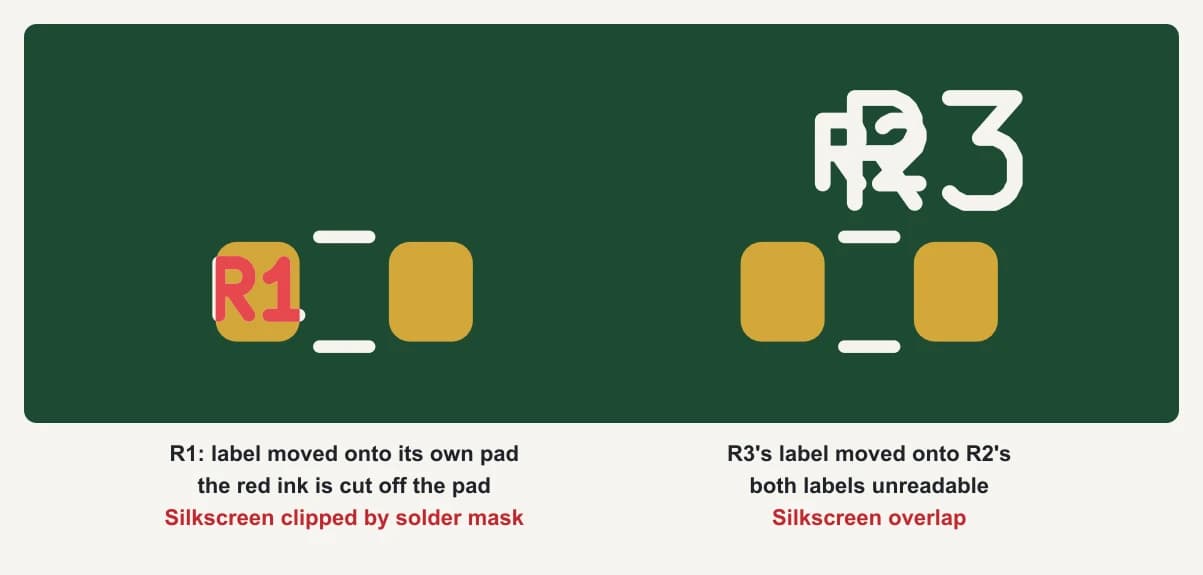
“Silkscreen clipped by solder mask” means part of the label sits inside a solder mask opening. Ink cannot go on copper that will be soldered, so that part is cut away and the label prints incomplete. JLCPCB asks for 0.15 mm between pads and silkscreen. “Silkscreen overlap” means two silkscreen items print on top of each other. Move the labels, or put the dense ones on the fabrication layer and keep the silkscreen for what someone holding the board needs to read.
How PCBEditor sizes its labels
PCBEditor draws every label with KiCad’s stroke font and the same cap, a line no wider than a quarter of the text size, so the line width on screen is the one in the fab files. A label’s line is 15% of its height, raised to the board’s minimum silkscreen width. Its rules check reports a label printed over a pad, using the label’s real strokes and the pad’s real outline. When you export to KiCad, Board Setup carries a 0.8 mm minimum text height and a minimum text thickness equal to the board’s silkscreen minimum, so KiCad checks the same numbers.
It has no text height, text thickness or silkscreen overlap check of its own; after export, KiCad’s DRC is the one to read for those. The Gerber checklist covers what to look at on the silkscreen layer before ordering.
Common questions
- Why does KiCad say text thickness is out of range when my thickness is correct?
- KiCad draws a text line no wider than a quarter of the text's smaller dimension (width or height). At 0.5 mm, a typed 0.15 mm line is drawn 0.125 mm wide, and DRC checks the drawn width, so it reports “actual 0.125 mm”. Make the text at least four times the minimum line width (0.6 mm for 0.15 mm), or lower the minimum in Board Setup if your fab allows it.
- What is KiCad's default minimum text size?
- On a new KiCad 9 board, Board Setup → Design Rules → Constraints sets a minimum text height of 0.8 mm and a minimum text thickness of 0.08 mm. Both apply to silkscreen text only and are reported as warnings. New silkscreen text defaults to 1.0 mm with a 0.1 mm line; library footprint references are 1.0 mm with a 0.15 mm line.
- How do I change the size of all reference designators in KiCad?
- Edit → Edit Text & Graphics Properties opens a dialog that edits many items at once. Tick Reference designators (and any other footprint fields you want), enter the new size and line width, or use Set to layer default values, then apply. A short pcbnew Python script does the same from the command line.
- What is the smallest silkscreen text a PCB fab can print?
- Check your fab's capabilities page. JLCPCB lists a 0.15 mm minimum line width and 1.0 mm minimum text height; PCBWay lists 0.15 mm and 0.8 mm. Smaller text may still print but is not guaranteed to be readable.
- Why does KiCad say text height out of range?
- The text is shorter than the minimum text height in Board Setup → Design Rules → Constraints, 0.8 mm by default. The check applies to silkscreen text; the same small text on a copper or fabrication layer is not reported. Enlarge the text, move it to a fabrication layer, or lower the minimum to what your fab supports.
- What does “Silkscreen clipped by solder mask” mean in KiCad?
- Part of a silkscreen item lies inside a solder mask opening, usually a pad. The fab cannot print ink on bare copper that will be soldered, so that part is cut from the silkscreen and the label prints incomplete. Move the label off the pad.
Let PCBEditor place the labels
The editor opens with this board described in the chat box. Its labels are drawn with the same quarter-of-the-size cap, so what you see is the width that gets printed, and its rules check flags a label printed over a pad.
Open the board in the editor→Sources
DRC reports are kicad-cli’s text output for the item named, with unrelated lines removed. Figures are drawn from the pad outlines and text strokes KiCad generates for each board.
- KiCad 9.0.9 kicad-cli pcb drc, run on the six test boards described on this page (built with the pcbnew Python API: three R_0603_1608Metric resistors from the KiCad 9 library, references 0.5, 0.6 and 1.0 mm tall, Board Setup minimums set per board).
- KiCad 9.0.9 pcbnew: the drawn line width of 11 text sizes, the default text sizes and minimums of a new board, the library footprint's text, and dialog text (Minimum text height; Minimum text thickness; Edit Text & Graphics Properties; Reference designators; Set to layer default values; Text thickness is too large for the text size).
- JLCPCB, PCB capabilities, Legend section (read 7 November 2026): minimum line width 0.15 mm, minimum text height 1.0 mm (40 mil), width to height ratio 1:6, pad to silkscreen 0.15 mm.
- PCBWay, PCB capabilities (read 7 November 2026): minimum character width 0.15 mm, minimum character height 0.8 mm, width to height ratio 1:5.
- KiCad forum, 6 November 2026: “Warning: Text thickness out of range (min thickness 0.15mm; actual .125mm)”, reported on KiCad 10.0.8.