KiCad global label vs net label vs hierarchical label: what each one connects
You split a schematic into two sheets, put a label called SDA on each, and the sensor never sees the bus. KiCad has three kinds of label, and they differ in one thing: how far the name reaches. We drew the same I2C bus across two sheets with each kind, ran KiCad 9’s electrical rule check (ERC) and netlist on every version, and wrote down what came out.
Last reviewed
Short answer
A net label (KiCad’s menu calls it that; it is also called a local label, hotkey L) connects wires with the same name on the same sheet only. A global label (Ctrl+L) connects every global label with the same name on every sheet. A hierarchical label (H) connects a sub-sheet to the sheet pin of the same name on its sheet symbol in the parent sheet. Power symbols such as +3V3 and GND are global. Use net labels within a sheet, hierarchical labels for what a sheet passes to its parent (always for a sheet you place more than once), and global labels for the few signals every sheet shares.
Three labels, three reaches
A label gives a wire a name, and wires with the same name are connected without a wire between them. What differs between KiCad’s labels is where else that name counts. In KiCad’s menus the plain label is “Place Net Labels”, which is why people search for “net label vs global label”; the manual and the file format call the same thing a local label.
| Label | Place with | Connects | Net name in our test |
|---|---|---|---|
| Net label (local label) | L | Wires with the same name on the same sheet only | /SDA on the root sheet, /Sensor/SDA on the sub-sheet |
| Global label | Ctrl+L | Every global label with the same name, on every sheet | SDA |
| Hierarchical label | H, plus a sheet pin of the same name on the parent sheet | A sub-sheet’s net to the matching sheet pin on its sheet symbol | /Sensor/SDA, or /SDA once the root wire has a net label |
| Power symbol | P | Every power symbol with the same value, on every sheet | +3V3 |
KiCad 9 has one more kind, the directive label, which attaches a net class or other properties to a net. In the manual’s words they behave like labels except that they cannot be used to name a net. Hierarchical sheets themselves are drawn with S.
The test: one I2C bus on two sheets
The root sheet holds a 4-pin header, J1, with +3V3, SDA, SCL and GND. A sub-sheet called Sensor holds a BME280 wired as Bosch’s datasheet shows for I2C: CSB tied to VDDIO, which selects I2C; SDO pulled low, which sets address 0x76 (Bosch says SDO must not be left floating); 100 nF on VDD and on VDDIO; and 4.7 kΩ pull-ups on SDA and SCL. The circuit is the same in every version. Only the labels on SDA and SCL change.
Each version was checked with KiCad 9.0.9’s command-line tools: the electrical rule check with every severity on, and the netlist, which says which pins each net really joins.
Net labels stop at the sheet edge
First the version most people draw: a net label SDA at the end of the header’s wire, and another net label SDA at the end of the sensor’s wire on the other sheet.
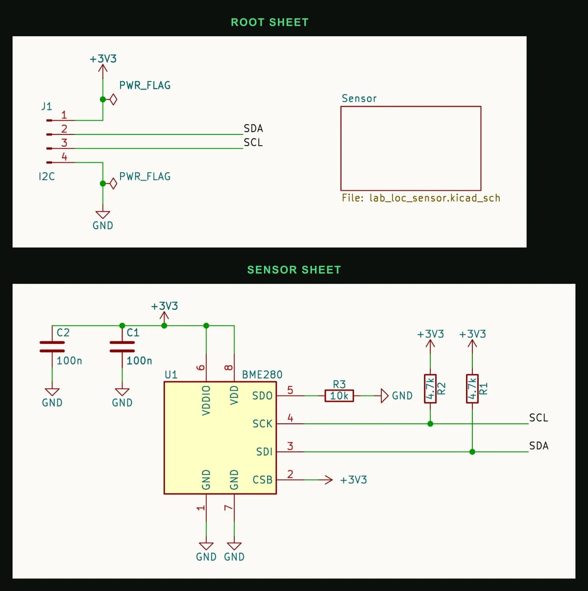
KiCad’s netlist has four signal nets where you meant two. /SDA holds J1 pin 2 and nothing else; /Sensor/SDA holds U1 pin 3 and R1. The slash and sheet name in front are KiCad saying the name belongs to that sheet. ERC reports this:
***** Sheet /
[label_dangling]: Label not connected to anything
    ; error
    @(60.96 mm, 50.80 mm): Label 'SDA'
[label_dangling]: Label not connected to anything
    ; error
    @(60.96 mm, 53.34 mm): Label 'SCL'

***** Sheet /Sensor/

 ** ERC messages: 2  Errors 2  Warnings 0
The labels are wired to J1, so “not connected to anything” reads oddly, and it is the message people search for. In this test KiCad flagged the labels that were alone on a net with one pin. The sub-sheet’s labels, each on a net with two pins, got no message, and nothing in the report mentions the label of the same name on the other sheet. We then added a pull-up on each of the header’s wires, so both halves had two pins: the bus was still split in two, and ERC reported 0 errors and 0 warnings.
Global labels: one net on every sheet
Change both pairs to global labels (Ctrl+L) and the bus joins. KiCad draws them as flags, which makes them easy to tell from net labels at a glance.
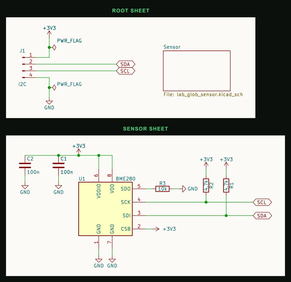
The netlist now has one net per signal: SDA joins J1 pin 2, R1 and U1 pin 3, and the name has no sheet path in front because it belongs to the whole design. ERC: 0 errors, 0 warnings. Power symbols work the same way: every +3V3 symbol on every sheet is one net, which is why the sensor sheet gets its supply without a wire to the header.
Hierarchical labels and sheet pins
A hierarchical label (H) connects a sub-sheet to the one sheet symbol that uses it. It needs a partner on the parent sheet: a sheet pin with the same name on the sheet symbol, which you then wire like any pin. The manual is plain about it: a sheet pin’s name has to match the corresponding hierarchical label in the sub-sheet. The Sync Sheet Pins tool, on the sheet symbol’s right-click menu, lists labels without pins and pins without labels and adds the missing ones.
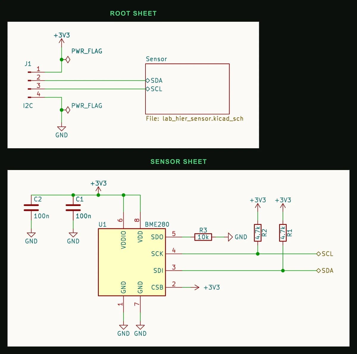
One net per signal again, this time through the sheet symbol, and ERC is clean. KiCad named the net /Sensor/SDA, because the only label on it is on the sub-sheet. Put a net label SDA on the root sheet’s wire and the same net becomes /SDA: a net takes its name from the highest sheet where it has a label. Leave the sheet pins off, and the sub-sheet’s labels are reported:
***** Sheet /Sensor/
[hier_label_mismatch]: Hierarchical label SCL has no matching sheet pin in the parent sheet
    ; error
    @(132.08 mm, 60.96 mm): Hierarchical Label 'SCL'
[hier_label_mismatch]: Hierarchical label SDA has no matching sheet pin in the parent sheet
    ; error
    @(132.08 mm, 66.04 mm): Hierarchical Label 'SDA'
A sheet pin and a global label are not alternatives for the same job: the pin is the parent’s half of a hierarchical label. If you searched for “global label vs sheet pin”, the comparison you want is global labels against hierarchical labels, below.
A sheet placed twice: where global labels go wrong
Hierarchical sheets can be placed more than once: two copies of the sensor, two motor drivers, eight LED channels. KiCad gives each copy its own references, and net labels and hierarchical labels give each copy its own nets (in our test, /Sensor1/SDA and /Sensor2/SDA). Global labels are different: a global label is the same net wherever it appears, including in every copy of a sheet. We placed the Sensor sheet twice, once with hierarchical labels and a header for each copy, and once with global labels:
Hierarchical labels, sheet placed twice (ERC: 0 errors, 0 warnings)
  /Sensor1/SDA   J1.2  R1.2  U1.3
  /Sensor2/SDA   J2.2  R101.2  U101.3

Global labels, sheet placed twice (ERC: 0 errors, 0 warnings)
  SDA            J1.2  R1.2  R101.2  U1.3  U101.3
With hierarchical labels each sensor has its own bus. With global labels both sensors and both pairs of pull-ups land on one SDA net, and ERC reports nothing, because nothing is wrong electrically as far as it can tell. On the board, both BME280s answer at 0x76 on the same bus, and two 4.7 kΩ pull-ups in parallel make 2.35 kΩ.
Global labels inside a reused sheet
Global label vs hierarchical label: which to use
- Net labels for anything that stays on one sheet. They name a net and save long wires across the page.
- Hierarchical labels for what a sheet passes to its parent. The sheet symbol then shows the block’s connections, the way a chip’s symbol shows its pins, and a sheet placed twice keeps its copies apart.
- Global labels for the few signals that really are everywhere in a flat design, such as a reset line or one I2C bus that every sheet taps. Use power symbols for supply rails.
- One kind per net. A net label SDA on one sheet and a global label SDA on another make two nets, and KiCad warns “Local and global labels have same name”.
ERC will not always catch a split, so check what a label actually joined: hover over a wire and press the backtick key (Highlight Net) to light up the whole net on every sheet, or read the netlist.
The ERC messages about labels
Every message below came from one of our test projects, with KiCad 9’s default severity. KiCad 9 also has “Global label only appears once in the schematic”, which is switched off by default.
| Message | Severity | What caused it | Fix |
|---|---|---|---|
| Label not connected to anything | Error | A net label alone on a net with one pin. The same name on another sheet does not count. | Use a global or hierarchical label, or wire the net on this sheet |
| Hierarchical label SDA has no matching sheet pin in the parent sheet | Error | A hierarchical label whose sheet symbol has no pin of that name | Add the pin with Sync Sheet Pins, then wire it |
| Global label not connected anywhere else in the schematic | Warning | A global label on a net with fewer than two pins: the only label of its name, or one that misses its wire | Check the spelling and that the label sits on the wire’s end |
| Labels are similar (lower/upper case difference only) | Warning | SDA on one sheet, sda on the other: two nets | Use one spelling |
| Local and global labels have same name | Warning | A net label SDA and a global label SDA: two nets | Use one kind of label for the net |
| Both SDA and I2C_SDA are attached to the same items; SDA will be used in the netlist | Warning | Two names on one wire; the global label’s name wins | Keep one name |
| Pin not connected, with Unconnected wire endpoint | Error and warning | A label one grid step (1.27 mm) past the end of its wire | Move the label onto the wire’s end |
The last row is worth a second look. A label connects only at its connection point, the end of the label that touches the wire. Moved one grid step past the wire’s end, the global label SCL joined nothing, the header’s SCL wire ended in the air, and KiCad reported J1 pin 3 as not connected. The SCL net then held only the sensor and its pull-up.
Labels are case-sensitive: SDA and sda are two nets. KiCad warns about that one; it does not warn about SDA and I2C_SDA on different wires, which are simply two different names.
Bringing a KiCad project into PCBEditor
PCBEditor imports KiCad projects: the .kicad_pcb with every .kicad_sch, or the zipped project. Its schematic import reads labels by KiCad’s rules: net labels within their sheet, global labels and power symbols across sheets, hierarchical labels to their sheet pins, and a sheet placed more than once gets its own nets and references per copy. We ran all thirteen test projects through it, and every net held the same pins as in KiCad’s own netlist. It leaves out nets with a single pin and names nets without the sheet path.
That also means it imports what you drew. A bus split by net labels on two sheets comes in split, and two copies joined by global labels come in joined. Run KiCad’s ERC before you import and read every label message; the power pin page covers the other ERC errors new KiCad users meet first.
Common questions
- What is the difference between a global label and a net label in KiCad?
- Reach. A net label, also called a local label (hotkey L), connects wires with the same name on the same sheet only. A global label (Ctrl+L) connects every global label of that name on every sheet of the design. In KiCad 9 a net label SDA on two sheets makes two nets, /SDA and /Sensor/SDA, while a global label SDA makes one net called SDA.
- How do I connect a net between sheets in KiCad?
- Either put a global label with the same name on both sheets, or put a hierarchical label (H) on the sub-sheet and a sheet pin of the same name on its sheet symbol in the parent sheet, then wire the pin. A net label alone does not leave its sheet.
- When should I use hierarchical labels instead of global labels?
- Whenever a sheet is a block with inputs and outputs, and always when the same sheet is placed more than once. Hierarchical labels give each copy its own nets. Global labels inside a reused sheet join every copy into one net, and KiCad's ERC reports nothing.
- Why does KiCad say “Label not connected to anything” when the label is on a wire?
- In our KiCad 9 test it flagged net labels that were alone on a net with one pin, a header pin whose other end was meant to be on another sheet. A net label with the same name on a different sheet is a different net, so the label really connects to nothing else. Use a global label or a hierarchical label with a sheet pin. With two pins on each half, the same split passed ERC with no message, so check with Highlight Net too.
- Are KiCad labels case-sensitive?
- Yes. In KiCad 9, global labels SDA and sda make two separate nets, and ERC warns “Labels are similar (lower/upper case difference only)”.
- What does “Global label not connected anywhere else in the schematic” mean?
- The global label is on a net with fewer than two pins: no other label of that name exists, or the label does not touch its wire, so the rest of the net is somewhere else. Check the spelling and the case, and that the label sits on the wire's end.
- What are the KiCad shortcuts for labels?
- In KiCad 9: L places a net label, Ctrl+L a global label, H a hierarchical label, S a hierarchical sheet and P a power symbol. Directive labels and sheet pins have no default key; sheet pins are easiest to add with Sync Sheet Pins.
Try the same BME280 board in PCBEditor
The editor opens with this sensor circuit described in the chat box. Change it to your own; PCBEditor draws the schematic, routes the board and checks it. You can also import a KiCad project there and keep going.
Open the BME280 board in the editor→Sources
The ERC reports are copied from kicad-cli’s text output; only the date line and report header are left out. The net lists show each net’s name and pins from KiCad’s netlist.
- KiCad 9.0 Schematic Editor manual (docs.kicad.org): Labels, Power Symbols, Net name assignment rules, Hierarchical Schematics (sheet pins and Sync Sheet Pins), the list of ERC checks with their default severities, and the Actions reference for the hotkeys.
- KiCad 9.0.9 kicad-cli sch erc and sch export netlist, run on thirteen two-sheet projects built for this page from KiCad’s own symbol library (Connector:Conn_01x04_Pin, Sensor:BME280, Device:R, Device:C, power:PWR_FLAG).
- Bosch Sensortec, BME280 datasheet BST-BME280-DS001, revision 1.24: section 6.1 (interface selection by CSB), section 6.2 (I²C address 0x76 or 0x77 set by SDO, which must not float), and Figure 17 (I²C connection diagram: 100 nF on VDD and VDDIO, pull-ups of normally 4.7 kΩ, CSB connected directly to VDDIO).