ESP32 LiPo charger circuit: MCP73831 or TP4056, load sharing and battery level
Charging a LiPo cell on an ESP32 board takes one charger chip and a resistor. The trouble is in what surrounds it: a charge current the cell or the USB port can’t take, a charger too hot to finish, a board that keeps the charge from ending, 4.2 V on a 3.6 V pin, and a battery reading that is off by a tenth of a volt. Here is a complete circuit for an ESP32-C3, drawn in KiCad, with the numbers taken from the datasheets.
Last reviewed
Short answer
Use a single-cell linear charger from USB 5 V: the MCP73831 up to 500 mA, or the TP4056 up to 1 A. One resistor sets the current; keep it at or below the cell’s 1C rate (500 mA for a 500 mAh cell). If the board runs while it charges, feed the 3.3 V regulator through a load-sharing path or a power-path charger such as the BQ24074, not straight from the cell. Never wire the cell or a charger module’s output to the ESP32’s 3.3 V pin: a full cell is 4.2 V and the chip is rated 3.0 to 3.6 V. To read the battery, use a 2.4 MΩ / 1 MΩ divider with 100 nF into an ADC1 pin.
The circuit
Four blocks, left to right: a USB-C input that asks the host for 5 V with one 5.1 kΩ per CC pin, the charger and the cell, a load-sharing path that picks USB or the cell for the rest of the board, and a 3.3 V regulator with the ESP32. A divider from the cell to an ADC pin reads the battery.
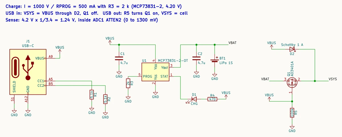
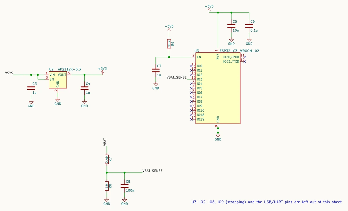
It is one KiCad 9 sheet, cropped in two. It passes the electrical rule check, and the netlist was read net by net: STAT drives the LED’s cathode, the cell and Q1’s drain share VBAT, and only VSYS feeds the regulator. The values for the module (decoupling and the EN delay) are the ones in Espressif’s ESP32-C3-WROOM-02 datasheet. Pick the cell’s connector polarity from the cell, not from the footprint: JST-PH leads are not wired the same way by every seller.
Which charger
All three are linear single-cell chargers with a constant-current, constant-voltage cycle. They differ in current, accuracy and whether they can run the board themselves.
| MCP73831 | TP4056 | BQ24074 | |
|---|---|---|---|
| Charge current | 15–500 mA | up to 1000 mA | up to 1.5 A |
| Set by | RPROG: 1000 V / R | RPROG: table | RISET: 890 AΩ / R |
| Charge voltage | 4.20 V ±0.75 % | 4.2 V (4.137–4.263) | 4.2 V |
| Input | 3.75–6 V | 4.0–8.0 V | 28 V rating, OVP 10.5 V |
| Runs the board while charging | no, add load sharing | no, add load sharing | yes, power path (OUT 4.4 V) |
| Package | SOT-23-5, DFN-8 | SOP-8 | VQFN-16, 3 × 3 mm |
- MCP73831 for a small cell and a USB port: a five-pin part, the tighter charge voltage, and a KiCad library symbol.
- TP4056 when you want 1 A, or when you are using a ready-made module. It has a TEMP pin for the cell’s thermistor; ground it to disable the check.
- BQ24074 when the board must run while it charges, or from a weak USB source. It powers the board and charges the cell at the same time, and limits what it draws from USB (100 mA or 500 mA, or a set limit).
Setting the charge current
On the MCP73831 the current is 1000 V divided by the PROG resistor, in kΩ and mA: 2 kΩ gives 500 mA, 10 kΩ gives 100 mA. On the TP4056 use the datasheet’s table:
| RPROG (kΩ) | 10 | 5 | 4 | 3 | 2.4 | 2 | 1.5 | 1.2 |
|---|---|---|---|---|---|---|---|---|
| Charge current (mA) | 130 | 250 | 300 | 400 | 500 | 580 | 780 | 1000 |
Three limits decide the value, and the lowest wins:
- The cell. Microchip’s datasheet gives the usual rule: 1C preferred, 2C absolute maximum. A 500 mAh cell charges at 500 mA; a 150 mAh cell at 150 mA, which on a TP4056 means about 10 kΩ, not the 1.2 kΩ of a 1 A setting.
- The USB port. The board draws from the same 5 V while it charges. An ESP32-C3 peaks at 335 mA while transmitting, so a 500 mA charge plus a working board is more than a 500 mA port gives. Charge slower, or use the BQ24074, which limits the input and gives the board priority. The CC resistors only ask the host for its default current.
- Heat, below.
Heat: why the charge slows down
A linear charger drops the difference between the input and the cell across itself. The worst moment is just after the cell leaves the trickle phase: the cell is near 3 V and the current is at full.
- MCP73831: Microchip’s own example is (5.5 V − 2.7 V) × 550 mA = 1.54 W. In the SOT-23-5, rated 230 °C/W on a standard board (130 °C/W or better with large copper), that is well past what it can shed, and the chip enters thermal regulation. The DFN package is rated 76 °C/W.
- TP4056: (5 V − 3.0 V) × 1 A = 2 W in an SOP-8. It holds its junction at 145 °C by cutting the current.
Neither fails; the current drops and the charge takes longer. If the board is meant to charge at the full set current, give the chip copper: a pour on the thermal pad or the ground pins, with vias to an inner or bottom plane.
A hot charger near the cell
Running the board while it charges
A simple charger ends the charge when its current falls to a set fraction of the programmed current (C/10 on the TP4056, an option between 5 % and 20 % on the MCP73831). If the board hangs on the cell, its draw is part of that current, and a board drawing more than the threshold keeps the charge from ever ending.
The fix in the first figure is Microchip’s AN1149 load-sharing path. With USB present, VSYS comes from VBUS through D2, and Q1’s gate sits at 5 V, above its source, so Q1 is off and the charger sees only the cell. Unplug USB and R5 (100 kΩ) pulls the gate to ground; Q1 turns on and VSYS comes from the cell. Two choices matter:
- Q1 must turn fully on with only the cell’s voltage across its gate, about 3 V near the end of the charge. Read its on-resistance at a gate-source voltage of 2.5 V in its datasheet, not at 10 V.
- D2 carries the whole board while USB is in. Rate its average current above the board’s (the ESP32-C3-WROOM-02 asks for a supply that delivers 0.5 A), and expect VSYS a few hundred millivolts below VBUS.
VSYS then runs from about 3.0 V (cell nearly empty) to about 4.7 V (USB). The AP2112K-3.3 accepts 2.5 to 6.0 V; what it does near the bottom of the cell is the dropout question in 3.3 V from a LiPo cell. The BQ24074 does all of this inside one chip: it holds its output at 4.4 V from USB, charges with what is left, and switches to the cell when USB goes away.
Wiring a TP4056 module to an ESP32
A TP4056 module with protection has B+ and B− for the cell and OUT+ and OUT− for the load. OUT+ is the cell voltage, 3.0 to 4.2 V, not a regulated rail. Two wirings are common, and both go wrong:
- OUT+ to the dev board’s 3V3 pin. A full cell puts 4.2 V on a chip rated 3.0 to 3.6 V. It may run for a while; it is outside the rating every time the cell is above 3.6 V.
- OUT+ to the dev board’s 5V pin. Within ratings, but the cell then goes through the dev board’s own regulator, which may need more headroom than a LiPo has, and the board resets as the cell drops. Check that regulator’s dropout in its datasheet; the arithmetic is in 3.3 V from a LiPo cell.
On a custom board, wire OUT+ to the input of a low-dropout 3.3 V regulator (or a buck-boost converter), as in the second figure. Also check the PROG resistor on the module against the table above; 1.2 kΩ means 1 A.
If the module carries a protection IC such as the DW01A, it cuts the cell off at 4.30 V (overcharge) and 2.40 V (overdischarge), and reconnects at 4.10 V and 3.00 V. Treat 2.40 V as the last resort, not as your low-battery cut-off. Set your own in firmware, well above it, and go to deep sleep there.
Reading the battery on an ESP32-C3
The cell reaches 4.2 V and the ADC reads at most 2.5 V, so it needs a divider. Three numbers from Espressif’s datasheet decide its values:
- The pin. ADC1 is on GPIO0 to GPIO4 and is factory-calibrated. GPIO0 and GPIO1 double as the 32 kHz crystal pins, GPIO2 is a strapping pin and GPIO4 is a JTAG pin, so GPIO3 is the free one. GPIO5 is ADC2: not calibrated, and not working on some chip revisions.
- The range. At the 0–2500 mV setting the calibrated error is ±35 mV. At 0–1300 mV it is ±10 mV.
- The current. In deep sleep the chip draws 5 µA, so a divider that draws 21 µA (two 100 kΩ resistors) uses four times more than the chip itself.
| Divider | Pin at 4.2 V | ADC range | ADC error at the cell | Divider current |
|---|---|---|---|---|
| 100 kΩ / 100 kΩ | 2.10 V | 0–2500 mV | ±70 mV | 21 µA |
| 2.4 MΩ / 1 MΩ | 1.24 V | 0–1300 mV | ±34 mV | 1.2 µA |
The high-value divider halves the error and draws about seventeen times less. Its source impedance is about 0.7 MΩ, so C8 does the work at the moment of sampling: 100 nF at the pin holds the voltage while the ADC takes its sample, and it is the capacitor Espressif’s own ADC figures were measured with. After a big change, such as plugging in the cell, allow a few tenths of a second for it to settle.
The resistors are now the bigger error
Read the cell when the radio is idle. A transmit burst pulls the cell down for a moment, and the reading drops with it. A cell’s voltage is not a linear fuel gauge either: take the percentage from its datasheet’s discharge curve, or treat the voltage as three levels (full, fine, charge me).
Checks before you order the board
- The PROG (or ISET) resistor gives a current at or below the cell’s 1C rate and within the USB budget.
- Nothing on the 3.3 V rail can see the cell directly: every path from VBAT or OUT+ goes through the regulator.
- The regulator is fed from the load-sharing node (VSYS) or a power-path output, not from the charger’s cell pin, if the board runs while charging.
- Q1’s on-resistance is rated at a gate voltage the cell can give; D2’s current rating covers the whole board.
- The charger has copper for its heat, and the cell is not sitting on it.
- The cell connector’s polarity matches the cell you will buy.
- The divider is on an ADC1 pin, with 100 nF at the pin, and the firmware uses the 0–1300 mV range for a 2.4 : 1 divider.
- The module has its EN delay (10 kΩ and 1 µF on the ESP32-C3-WROOM-02) and its decoupling at the 3V3 pin.
For the rest of an ESP32 board (antenna keep-out, USB, strapping pins), see ESP32 PCB design.
Common questions
- Can I connect a TP4056 module’s output to the ESP32 3.3 V pin?
- No. The output is the cell itself, up to 4.2 V when full, and the ESP32-C3 is rated 3.0 to 3.6 V. Put a 3.3 V regulator between them, ideally fed through a load-sharing path so the board can run while the cell charges.
- How do I set the TP4056 charge current?
- With the resistor from PROG to GND. The datasheet’s table gives 1000 mA at 1.2 kΩ, 500 mA at 2.4 kΩ, 300 mA at 4 kΩ and 130 mA at 10 kΩ. Keep the current at or below your cell’s 1C rate.
- What charge current should I use for a LiPo?
- At most what the cell’s datasheet allows. Microchip’s charger datasheet gives the usual rule: the preferred fast-charge current is the 1C rate (500 mA for a 500 mAh cell), with 2C as the absolute maximum. Also count the board’s own current against what the USB port supplies.
- Can the ESP32 run while the LiPo is charging?
- Yes, but not from the cell node of a simple charger. The charger ends the charge when its current falls to a fraction of the set current, and the board’s draw keeps it from getting there. Use a load-sharing path (a Schottky from USB and a P-channel MOSFET from the cell) or a charger with a power path such as the BQ24074.
- Which ESP32-C3 pin should I use to read the battery voltage?
- An ADC1 pin: GPIO0 to GPIO4 are ADC1 and factory-calibrated. GPIO0 and GPIO1 are the 32 kHz crystal pins, GPIO2 is a strapping pin and GPIO4 is a JTAG pin, which leaves GPIO3 the easy choice. Avoid GPIO5 (ADC2): it is not calibrated and does not work on some chip revisions.
- Why does my charger get hot?
- A linear charger burns the difference between USB and the cell as heat: (5 V − 3.0 V) × 1 A is 2 W in a TP4056. Both chips then cut the current to protect themselves, so the charge just takes longer. Give the chip copper, or charge at a lower current.
Start this battery board from its description
The editor opens with this circuit described in the chat box: USB-C, the MCP73831 at 500 mA, load sharing, the AP2112K-3.3, an ESP32-C3 and the battery divider. Change the values to your cell.
Open the ESP32 battery board in the editor→Sources
Cell limits (charge current, voltage, temperature) come from your own cell’s datasheet; the 1C rule is a default, not a promise.
- Microchip, MCP73831/2 datasheet (DS20001984H): 15–500 mA, IREG = 1000 V / RPROG (2 kΩ: 450–550 mA); MCP73831-2 regulation 4.20 V (4.168–4.232 V); VDD 3.75–6 V; SOT-23-5 θJA 230 °C/W (130 °C/W or better with large copper), DFN 76 °C/W; the 1.54 W worked example; thermal shutdown 150 °C; 1C preferred, 2C absolute maximum.
- Microchip, AN1149: a load-sharing path for its stand-alone Li-ion chargers (P-channel MOSFET, Schottky diode, 100 kΩ gate pull-down), worked with the MCP73837.
- NanJing Top Power, TP4056 datasheet: input 4.0–8.0 V; float 4.137–4.263 V (4.2 V typical); the RPROG table (1.2 kΩ: 950–1050 mA; 2.4 kΩ: 450–550 mA); 2.9 V trickle threshold; C/10 termination; TEMP pin; constant-temperature mode at 145 °C.
- Texas Instruments, BQ2407x datasheet: up to 1.5 A charge, dynamic power path management, BQ24074 input overvoltage 10.5 V and system output 4.4 V, 28 V input rating, ICHG = KISET / RISET (KISET 890 AΩ typical), selectable 100 mA / 500 mA USB input limit, VQFN-16 3 × 3 mm.
- Fortune Semiconductor, DW01A datasheet (DW01A-DS-10): overcharge 4.30 V (release 4.10 V), overdischarge 2.40 V (release 3.00 V), overcurrent 150 mV, supply current 3.0 µA typical.
- Espressif, ESP32-C3 Series datasheet v2.4: ADC1 on GPIO0–GPIO4 (factory-calibrated), ADC2 on GPIO5; effective ranges and total error per attenuation (Table 5-6); 100 nF in the ADC test condition; Deep-sleep 5 µA; 335 mA peak (802.11b transmit at 21 dBm); 3.0–3.6 V supply; strapping pins GPIO2, GPIO8, GPIO9.
- Espressif, ESP32-C3-WROOM-02 datasheet v1.7: 3.0–3.6 V, a supply that delivers at least 0.5 A, EN RC of 10 kΩ and 1 µF, 10 µF + 0.1 µF on 3V3.
- Diodes Incorporated, AP2112 datasheet (DS39724 Rev. 2): 600 mA, input 2.5–6.0 V.