ESP32-P4 vs P4X: what chip revision v3.x changes on your PCB
Espressif’s current ESP32-P4 parts end in X, the development boards are now called P4X, and a board laid out for the first P4 silicon does not simply take the new chip. Three parts of the circuit changed between chip revision v1.x and v3.x, and the firmware has to be rebuilt. Here is each change with Espressif’s values, drawn in KiCad 9.
Last reviewed
Short answer
“P4X” is the ESP32-P4 at chip revision v3.x: Espressif’s datasheet lists ESP32-P4NRW16X and ESP32-P4NRW32X, both v3.x, and its P4X development boards carry v3.1 or later. On the PCB, three things change from v1.x: pin 54 goes from NC to VDD_HP_1 and needs the 1.1 V core supply with a 0.1 µF capacitor; the external DC/DC’s feedback gets two 499 kΩ resistors and a 22 pF capacitor; and the 1 MΩ pull-down on USB_DP is no longer needed. Firmware must be built with ESP-IDF v5.5.3 or later (or v6.0) for v3.x.
What the X means
The ESP32-P4 datasheet (pre-release v0.7) now lists two parts, ESP32-P4NRW16X and ESP32-P4NRW32X, with 16 MB and 32 MB of PSRAM in the package, and gives both as chip revision v3.x. Espressif’s chip revision v3.x user guide names the same two as its related products. The development boards follow: Espressif’s documentation gives one difference between the ESP32-P4X-Function-EV-Board and the ESP32-P4-Function-EV-Board, the main chip, which is chip revision v3.1 or later on the P4X board. The ESP32-P4X-EYE and ESP32-P4X-C5-Function-EV-Board carry the same X.
What the X itself stands for, Espressif does not write down. The datasheet’s nomenclature explains every other letter (N for normal-temperature PSRAM, R for PSRAM, W for 16-line 1.8 V PSRAM, the number for the PSRAM size in MB) and stops there. The same datasheet also says that several chip revisions can be on the market under the same part number. So read the X as “the v3.x part” when you order, and confirm the revision on the chip itself, as shown below.
Revision v3.x is a large change inside the chip: the high-performance RISC-V cores go from 360 MHz to 400 MHz, and for v3.1 Espressif counts more than 50 hardware and register changes, in the ISP, the CPU, memory, the flash and PSRAM interface and the security blocks among others. For a board designer, three of them reach the PCB.
The three board changes at a glance
| What | v1.0 / v1.3 | v3.0 and later | What to do |
|---|---|---|---|
| Pin 54 | NC (no connection) | VDD_HP_1, a digital supply pin (0.99 to 1.3 V) | Feed it from ESP_VDD_HP; Espressif uses a 0 Ω (R39) and 0.1 µF (C39) at the pin |
| DC/DC feedback (FB_DCDC) | R1, R2 and C2 as empty pads | R1 = R2 = 499 kΩ, C2 = 22 pF across R1 | Fit all three; Espressif says they must be populated |
| 1 MΩ on USB_DP | Fitted, to stop a current surge on VDD_USBPHY when CHIP_PU goes low | Not needed (the fault is fixed) | Optional; you may keep it so one layout suits both |
| Firmware | ESP-IDF builds for v1.x | ESP-IDF v5.5.3 or later, or v6.0 or later, built for v3.x | Rebuild; one image cannot serve both revisions |
Espressif marks v1.0 and v1.3 “not recommended for new designs” throughout its hardware design guidelines, and the reference schematic for v3.0 and later is the one to start from.
The DC/DC feedback: 499 kΩ, 499 kΩ, 22 pF
The P4’s high-performance core does not run from your 3.3 V rail. Its four VDD_HP pins take 0.99 to 1.3 V (1.1 V typical) from an external step-down converter, and the chip controls that converter itself through two pins: EN_DCDC (pin 79) switches it on once the firmware starts, and FB_DCDC (pin 78) goes to the converter’s feedback pin. Espressif’s example is a TLV62569 with 4.7 µF in, a 2.2 µH inductor and 22 µF out.
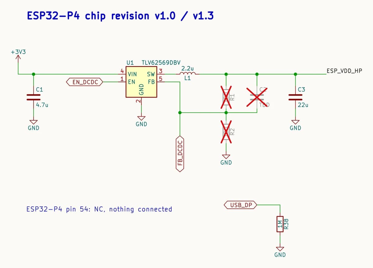
On v1.x, the feedback resistors and capacitor were optional. Espressif’s v1.x schematic shows R1, R2 and C2 as TBD(NC) with a note not to mount them by default, and the guidelines asked designers to keep the pads anyway.
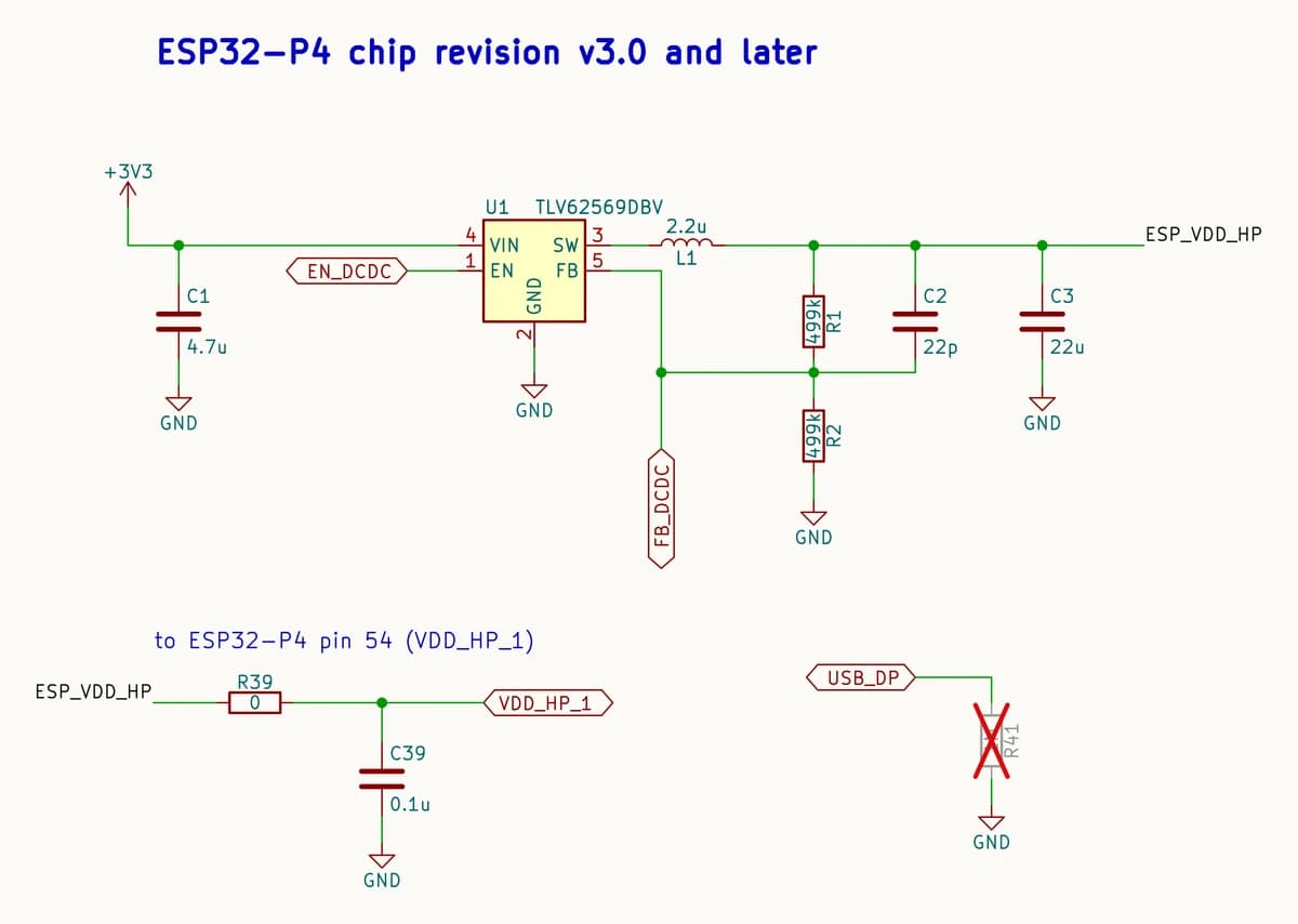
On v3.0 and later, Espressif writes that the feedback resistor and feedback capacitor must be populated: R1 = 499 kΩ from the DC/DC output (ESP_VDD_HP) to FB_DCDC, R2 = 499 kΩ from FB_DCDC to ground, and C2 = 22 pF across R1. With its own TLV62569 values unchanged, that is the whole DC/DC difference. If you use another converter, pick it from Espressif’s verified list (ETA3485, SY8088, RY3420, BL8028, LP3219 or TLV62569), take its input and inductor from its own datasheet, and place it close to the P4, which the reference schematic stresses.
Leave EN_DCDC to the chip
Pin 54 becomes VDD_HP_1
On v1.0 and v1.3, pin 54 of the QFN104 package is NC. From v3.0 it is VDD_HP_1, one of the four high-performance supply pins: VDD_HP_0 is pin 26, VDD_HP_1 pin 54, VDD_HP_2 pin 76 and VDD_HP_3 pin 91. All four take the same ESP_VDD_HP rail.
Espressif’s v3.0 reference schematic feeds pin 54 from ESP_VDD_HP through a 0 Ω resistor (R39) and puts a 0.1 µF capacitor (C39) right at the pin, the same 0.1 µF each VDD_HP pin gets; pin 26 also has the 10 µF bulk capacitor. On a layout, that means a trace or plane connection from the core supply to pin 54 and a decoupling capacitor beside it, at a pin that used to have nothing.
The 1 MΩ on USB_DP
The P4’s high-speed USB 2.0 OTG pins are USB_DM (pin 49) and USB_DP (pin 50). On v1.0 and v1.3, Espressif adds a 1 MΩ pull-down on USB_DP to stop a large transient current on VDD_USBPHY when CHIP_PU is pulled low. In v3.0 and later that is fixed, and Espressif allows the 1 MΩ to stay for design compatibility. Its v3.0 schematic draws it as R41, 1M(NC).
A related v1.x fix also goes away: on v1.0 and v1.3, VDD_USBPHY leaks current in low-power modes and Espressif recommends a MOSFET to switch it off. In v3.0 that is fixed too, and the 0 Ω in series with VDD_USBPHY can stay.
Will a v3.x chip work on my v1.x board?
Not without changes. Two of the three are part changes: fit R1, R2 and C2 on the pads Espressif told you to keep, and the 1 MΩ on USB_DP can stay. Pin 54 is the problem. A v1.x layout had no reason to route it, so on most boards the pad connects to nothing, and v3.x needs it on the core supply with a capacitor beside it. That is a layout change: plan a new board revision.
Distributors may not say which revision you get
Which revision is on my board?
The manufacturing code line in the chip marking gives the revision. From Espressif’s errata, chip revision identification:
| Chip revision | Manufacturing code |
|---|---|
| v1.0 | X C XX |
| v1.3 | X E XX |
| v3.0 | X F XX |
| v3.1 | X G XX |
| v3.2 | X H XX or X J XX |
In software the revision is in eFuse: the major number in EFUSE_RD_MAC_SPI_SYS_2_REG bits 23, 5 and 4, the minor number in bits 3 to 0. esptool reads it and prints the chip revision when it connects. In Espressif’s vM.X scheme, a change in M means software for the old revision does not run on the new one, which is why v1.x and v3.x need separate builds.
Firmware: ESP-IDF v5.5.3 and the revision option
Chip revision v3.x needs ESP-IDF v5.5.3 or later, or v6.0 or later. Those versions add one option to sdkconfig, CONFIG_ESP32P4_SELECTS_REV_LESS_V3: n, the default, builds for v3.x; y builds for v1.x. A project started on an in-between ESP-IDF version may still carry CONFIG_ESP32P4_SELECTS_REV_LESS_V3=y, and then the firmware either fails to download to a v3.x chip or fails to boot after flashing. Set it to n and rebuild.
Espressif is explicit that the two revisions cannot share one firmware image. If your product ships with both, build and track two images.
A v3.x power checklist
For the rest of a new v3.x board’s power circuit, these are the numbers from Espressif’s schematic checklist:
| Rail or pin | What Espressif asks for |
|---|---|
| Supply | 3.3 V single supply recommended; at least 380 mA for the chip with its flash and PSRAM, plus what your peripherals draw; 10 µF at each power entrance |
| VDD_HP_0 to VDD_HP_3 (pins 26, 54, 76, 91) | 0.99 to 1.3 V from the external DC/DC (ESP_VDD_HP); 10 µF at the source, 0.1 µF at each pin |
| VDD_LDO and VDD_DCDCC | 3.0 to 3.6 V; 10 µF on each trace and 0.1 µF at each pin. The DC/DC input is the same supply as VDD_DCDCC |
| External DC/DC | One of Espressif’s verified parts: ETA3485, SY8088, RY3420, BL8028, LP3219 or TLV62569, placed close to the chip, EN to EN_DCDC (pin 79), FB to FB_DCDC (pin 78) |
| VDD_USBPHY | 2.97 to 3.63 V, 10 nF + 0.1 µF + 4.7 µF; may float if you do not use the high-speed USB pins |
| VDD_MIPI_DPHY | 2.25 to 2.75 V from the internal regulator, 10 nF + 0.1 µF + 1 µF; may float without MIPI |
| VDD_BAT | 2.5 to 3.6 V, 0.1 µF + 10 µF; must not float |
| CHIP_PU | Must not float; RC delay of 10 kΩ and 1 µF as a starting point. Rails stable at least 50 µs before CHIP_PU rises; hold it low at least 1000 µs to reset |
The P4 has no radio. A P4 board that needs Wi-Fi or Bluetooth adds a second chip, as Espressif’s P4X-C5 board does with an ESP32-C5-MINI-1 module; for that part of the board, the ESP32 PCB design guide covers the antenna keep-out, power and USB rules.
Drawing an ESP32-P4 in KiCad
KiCad 9.0.9’s standard library has symbols for the ESP32-C3, ESP32-S2, ESP32-S3 and the PICO chips, and none for the ESP32-P4, so you will draw your own or bring one in. Build it from the current datasheet, not from a v1.x design:
- Pin 54 is
VDD_HP_1with the power-input pin type. A symbol made for v1.x marks it NC, and KiCad’s electrical rule check says nothing about an unconnected NC pin, so the mistake survives until the board does not boot. - Give FB_DCDC and EN_DCDC their own nets to the converter’s FB and EN pins. Neither goes to your 3.3 V rail.
- Put R1, R2 and C2 on the schematic with values, not as do-not-populate parts, and keep C39 beside pin 54 in the layout.
- If you keep the 1 MΩ on USB_DP so one layout suits both revisions, mark it do-not-populate for v3.x builds, and check that your bill of materials and position file leave it out.
The two figures above were drawn that way: KiCad’s own TLV62569DBV, resistor, capacitor and inductor symbols, Espressif’s values and reference designators, and KiCad’s DNP flag on the parts Espressif leaves unmounted. If KiCad reports power pins that nothing drives once the P4 symbol is in, the power pin page explains the fix.
Common questions
- What is the difference between ESP32-P4 and ESP32-P4X?
- The chip revision. The P4X parts (ESP32-P4NRW16X, ESP32-P4NRW32X) and the P4X development boards use ESP32-P4 chip revision v3.x, which runs its high-performance cores at up to 400 MHz instead of 360 MHz and fixes a list of v1.x errata. It also changes the board: pin 54 becomes the VDD_HP_1 supply pin, the DC/DC feedback needs two 499 kΩ resistors and a 22 pF capacitor, and firmware has to be rebuilt with ESP-IDF v5.5.3 or later.
- What does the X in ESP32-P4NRW16X stand for?
- Espressif does not say. The nomenclature in the ESP32-P4 datasheet (v0.7) explains N (normal-temperature PSRAM), R (PSRAM), W (16-line 1.8 V PSRAM) and the number (PSRAM size in MB), but not the trailing X. Both X parts are listed as chip revision v3.x, and the same datasheet notes that several revisions can be sold under one part number, so check the chip marking.
- Can I put an ESP32-P4 v3.x chip on a board designed for v1.x?
- Only if pin 54 can be fed. On v1.x pin 54 is NC, so most v1.x layouts leave it unrouted, while v3.x needs it on the 0.99 to 1.3 V VDD_HP supply with a 0.1 µF capacitor. The DC/DC feedback parts are easier: Espressif told v1.x designers to keep pads for R1, R2 and C2, so they can simply be fitted. Plan a new board revision unless pin 54 already reaches VDD_HP.
- How do I tell which ESP32-P4 chip revision I have?
- Read the manufacturing code on the chip: X C XX is v1.0, X E XX is v1.3, X F XX is v3.0, X G XX is v3.1, and X H XX or X J XX is v3.2. In software the revision is in eFuse (EFUSE_RD_MAC_SPI_SYS_2_REG bit 23 and bits 5 to 0), and esptool prints it when it connects.
- Which ESP-IDF version supports ESP32-P4 v3.x?
- ESP-IDF v5.5.3 or later, or v6.0 or later. Those versions add CONFIG_ESP32P4_SELECTS_REV_LESS_V3: n (the default) builds for v3.x, y builds for v1.x. A project created with an earlier ESP-IDF may still have it set to y, which makes the firmware fail to download to a v3.x chip or fail to boot, so set it to n and rebuild.
- Why does the ESP32-P4 DC/DC need 499 kΩ resistors on v3.x?
- Espressif’s v3.x reference circuit fits R1 = 499 kΩ from the DC/DC output to FB_DCDC, R2 = 499 kΩ from FB_DCDC to ground, and 22 pF across R1. FB_DCDC (pin 78) and EN_DCDC (pin 79) are driven by the ESP32-P4 itself to set and switch its 0.99 to 1.3 V core supply. On v1.x the same three parts were left unmounted; on v3.x Espressif says they must be populated.
- Is there an ESP32-P4 symbol in KiCad?
- Not in KiCad 9.0.9’s standard library, which has the ESP32-C3, S2, S3 and PICO chips but no P4. Draw your own from the current datasheet and give pin 54 the name VDD_HP_1 and a power-input type; a symbol copied from a v1.x design marks it NC, and KiCad’s ERC will not complain about an unconnected NC pin.
Bring the KiCad project into PCBEditor
PCBEditor opens KiCad projects in the browser: import the .kicad_pcb with its .kicad_sch files, or the zipped project, and the schematic’s nets come in by KiCad’s rules. Look at the board in 2D and 3D and run the design-rule check before you order.
Open the editor→Sources
Values and reference designators in the figures follow Espressif’s reference schematics; only the drawing is ours. The datasheet is a pre-release; check the current one before you order parts.
- Espressif, ESP32-P4 Chip Revision v3.x User Guide, v1.1 (2026.08): section 1 (design changes, 360 to 400 MHz, fixed errata), section 2.1 (hardware and software changes, CONFIG_ESP32P4_SELECTS_REV_LESS_V3), section 3 (v3.1 marking).
- Espressif, ESP32-P4 Series Datasheet, pre-release v0.7: Figure 1-1 (nomenclature), Table 1-1 (ESP32-P4NRW16X and ESP32-P4NRW32X, chip revision v3.x), section 1.3, Tables 2-11 and 2-12 (FB_DCDC, EN_DCDC and the VDD_HP pins), Table 5-2 (VDD_HP recommended input voltage).
- Espressif, ESP32-P4 Hardware Design Guidelines (docs.espressif.com, release master, 2026-11-03): section 1.3.1 and Figs. 1 and 2 (reference schematics for v3.0 and later and for v1.0/v1.3), section 1.3.2 (power supply, Figs. 5 and 6 for the TLV62569), section 1.3.3 (power-up and reset timing) and the USB section.
- Espressif, ESP Chip Errata, ESP32-P4 Chip Revision Identification: the vM.X numbering scheme, the eFuse bits and the manufacturing codes for v1.0 to v3.2.
- Espressif, esp-dev-kits, ESP32-P4X-Function-EV-Board user guide: hardware revision details (chip revision v3.1 or later).
- KiCad 9.0.9: the standard symbol library (Regulator_Switching:TLV62569DBV, Device:R, Device:C, Device:L) and kicad-cli schematic netlist and SVG export, used for the two figures.