ESP32-S31 pinout: every ESP32-S31-WROOM-3 pin, the boot pins, and which USB port is which
The ESP32-S31 is Espressif’s new dual-core RISC-V chip with Wi-Fi 6, Bluetooth 5.4 (LE and Classic), 802.15.4 for Zigbee and Thread, USB 2.0 high-speed and an Ethernet MAC. Boards built on it, such as Waveshare’s ESP32-S31-Zero, are starting to appear, and its datasheets are still marked pre-release. This page gives every pin of the ESP32-S31-WROOM-3 module from Espressif’s datasheet, drawn on Espressif’s own KiCad footprint, and what each special pin needs on your board. If you are coming from an ESP32-S3, the boot button has moved, and that is the first thing to change in a copied schematic.
Last reviewed
Short answer
The ESP32-S31-WROOM-3 has 99 pads and brings out 54 of the chip’s 60 GPIOs; GPIO26 to GPIO28 and GPIO30 to GPIO32 run the module’s flash, and the PSRAM is inside the chip package, so it takes no GPIOs. The boot button goes on IO61 (pad 71), not IO0: IO61 low with IO60 high at reset enters download mode. IO36 sets the flash voltage and is pulled up inside the module. Flash and debug over USB with IO33 (D−) and IO34 (D+), pads 42 and 43; USB_DP and USB_DM (pads 40 and 41) are the separate USB 2.0 high-speed OTG port. Feed 3V3 with at least 0.6 A.
The footprint, pad by pad
The WROOM-3 is 22.0 × 30.0 × 3.5 mm with pads on all four sides of a 0.85 mm grid. Pads 1 to 25 run down the left, 26 to 47 along the bottom, 48 to 72 up the right, and 73 to 94 across the top, just below the antenna. That top row is all ground except pad 91. Pad 95 in the middle is a ground pad made of nine squares, and pads 96 to 99 are the four corner grounds.
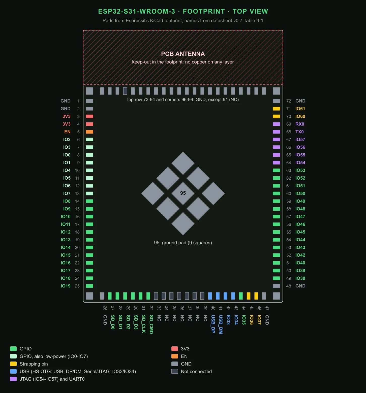
All 99 pins
Names and functions from Table 3-1 of the module datasheet. I²C and UART1 to UART3 have no fixed pins: the GPIO matrix routes them to any free GPIO. The fixed functions below matter for Ethernet, SDIO, the camera and LCD interfaces, the ADC and touch.
| Pad | Name | Function |
|---|---|---|
| 1, 2 | GND | Ground |
| 3, 4 | 3V3 | Supply, 3.0 to 3.6 V; the supply must deliver at least 0.6 A |
| 5 | EN | High enables the chip, low powers it off. Do not leave it floating |
| 6 | IO2 | GPIO2, LP_GPIO2, LP_UART_DTRN, LP_SPI_CK, LCD_DATA19_OUT |
| 7 | IO3 | GPIO3, LP_GPIO3, LP_UART_DSRN, LP_SPI_CS, LCD_DATA20_OUT |
| 8 | IO0 | GPIO0, LP_GPIO0, XTAL_32K_N (optional 32.768 kHz crystal). Not a boot pin on the S31 |
| 9 | IO1 | GPIO1, LP_GPIO1, XTAL_32K_P (optional 32.768 kHz crystal) |
| 10 | IO4 | GPIO4, LP_GPIO4, LP_UART_RTSN, LP_SPI_D, LCD_DATA21_OUT |
| 11 | IO5 | GPIO5, LP_GPIO5, LP_UART_CTSN, LP_SPI_Q, LCD_DATA22_OUT |
| 12 | IO6 | GPIO6, LP_GPIO6, TOUCH_CH0, LP_UART_TXD, LP_I2C_SCL |
| 13 | IO7 | GPIO7, LP_GPIO7, TOUCH_CH1, LP_UART_RXD, LP_I2C_SDA, LCD_DATA23_OUT |
| 14 | IO8 | GPIO8, TOUCH_CH2, GMAC_PHY_TXD0, LCD_DATA0_OUT |
| 15 | IO9 | GPIO9, TOUCH_CH3, GMAC_PHY_TXD1, LCD_DATA1_OUT, SPI2_HOLD |
| 16 | IO10 | GPIO10, TOUCH_CH4, GMAC_PHY_TXD2, LCD_DATA2_OUT, SPI2_CS |
| 17 | IO11 | GPIO11, TOUCH_CH5, GMAC_PHY_TXD3, LCD_DATA3_OUT, SPI2_D |
| 18 | IO12 | GPIO12, TOUCH_CH6, GMAC_PHY_TXEN, LCD_DATA4_OUT, SPI2_CK |
| 19 | IO13 | GPIO13, TOUCH_CH7, GMAC_RMII_CLK, LCD_DATA5_OUT, SPI2_Q |
| 20 | IO14 | GPIO14, TOUCH_CH8, GMAC_RX_CLK, LCD_DATA6_OUT, SPI2_WP |
| 21 | IO15 | GPIO15, TOUCH_CH9, GMAC_PHY_RXDV, LCD_DATA7_OUT, SPI2_IO4 |
| 22 | IO16 | GPIO16, TOUCH_CH10, GMAC_PHY_RXD3, LCD_DATA8_OUT, SPI2_IO5 |
| 23 | IO17 | GPIO17, TOUCH_CH11, GMAC_PHY_RXD2, LCD_DATA9_OUT, SPI2_IO6 |
| 24 | IO18 | GPIO18, TOUCH_CH12, GMAC_PHY_RXD1, LCD_DATA10_OUT, SPI2_IO7 |
| 25 | IO19 | GPIO19, TOUCH_CH13, GMAC_PHY_RXD0, LCD_DATA11_OUT, SPI2_DQS |
| 26 | GND | Ground |
| 27 | SD_D0 | SDIO_DATA0, GPIO20, SPI2_CK |
| 28 | SD_D1 | SDIO_DATA1, GPIO21, SPI2_D |
| 29 | SD_D2 | SDIO_DATA2, GPIO22, SPI2_Q |
| 30 | SD_D3 | SDIO_DATA3, GPIO23, SPI2_CS |
| 31 | SD_CLK | SDIO_CLK, GPIO24, SPI2_HOLD |
| 32 | SD_CMD | SDIO_CMD, GPIO25, SPI2_WP |
| 33 to 39 | NC | Not connected |
| 40 | USB_DP | USB 2.0 High-Speed OTG, D+ |
| 41 | USB_DM | USB 2.0 High-Speed OTG, D− |
| 42 | IO33 | USB Serial/JTAG D− by default; GPIO33, LCD_DATA12_OUT |
| 43 | IO34 | USB Serial/JTAG D+ by default; GPIO34, LCD_DATA13_OUT |
| 44 | IO35 | GPIO35, REF_GMAC_CLK, LCD_DATA14_OUT, SD2_CDATA0 |
| 45 | IO36 | Strapping: flash supply voltage. Pulled up inside the module. GPIO36, LCD_DATA15_OUT, SD2_CDATA1 |
| 46 | IO37 | Strapping: JTAG source, only read if an eFuse is burnt. No internal pull. GPIO37, LCD_DATA16_OUT, SD2_CDATA2, PAD_COMP0 |
| 47, 48 | GND | Ground |
| 49 | IO38 | GPIO38, LCD_DATA17_OUT, SD2_CDATA3, PAD_COMP1 |
| 50 | IO39 | GPIO39, LCD_DATA18_OUT, SD2_CCLK, PAD_COMP2 |
| 51 | IO40 | GPIO40, LCD_PCLK, SD2_CCMD, PAD_COMP3 |
| 52 | IO42 | GPIO42, ADC1_CH0_N |
| 53 | IO43 | GPIO43, ADC1_CH0_P, LCD_H_ENABLE |
| 54 | IO44 | GPIO44, ADC1_CH1_N, LCD_H_SYNC |
| 55 | IO45 | GPIO45, ADC1_CH1_P, LCD_V_SYNC |
| 56 | IO46 | GPIO46, ADC1_CH2_N, CAM_DATA0_IN |
| 57 | IO47 | GPIO47, ADC1_CH2_P, CAM_DATA1_IN |
| 58 | IO48 | GPIO48, ADC1_CH3_N, CAM_DATA2_IN |
| 59 | IO49 | GPIO49, ADC1_CH3_P, CAM_DATA3_IN |
| 60 | IO50 | GPIO50, ADC2_CH0_N, CAM_DATA4_IN |
| 61 | IO51 | GPIO51, ADC2_CH0_P, CAM_DATA5_IN |
| 62 | IO52 | GPIO52, ADC2_CH1_N, CAM_DATA6_IN, SPI2_CS |
| 63 | IO53 | GPIO53, ADC2_CH1_P, CAM_DATA7_IN, SPI2_CK |
| 64 | IO54 | MTDO (JTAG), GPIO54, ADC2_CH2_N, CAM_PCLK, SPI2_D |
| 65 | IO55 | MTCK (JTAG), GPIO55, ADC2_CH2_P, CAM_XCLK, SPI2_Q |
| 66 | IO56 | MTDI (JTAG), GPIO56, ADC2_CH3_N, CAM_V_SYNC, SPI2_HOLD |
| 67 | IO57 | MTMS (JTAG), GPIO57, ADC2_CH3_P, CAM_H_SYNC, SPI2_WP |
| 68 | TX0 | UART0_TXD, GPIO58. The UART0 used for flashing and the boot log |
| 69 | RX0 | UART0_RXD, GPIO59. The UART0 used for flashing and the boot log |
| 70 | IO60 | Strapping: boot mode and UART0 boot log. Weak pull-up. GPIO60 |
| 71 | IO61 | Strapping: boot mode. Weak pull-up; low at reset enters download mode. GPIO61 |
| 72 to 90, 92 to 99 | GND | Ground: the row under the antenna end, the four corners and the centre pad (95) |
| 91 | NC | Not connected (ANT2 on the WROOM-3U) |
Strapping pins: the boot button is on IO61
Four pins are read when EN goes high and latched until power-down. Espressif asks for them to hold their level for at least 3 ms after EN rises; after that they work as normal GPIOs.
| Pin | Default at reset | What it selects |
|---|---|---|
| IO61 (pad 71) | Weak pull-up (1) | Boot mode. High: boot from flash. Low with IO60 high: download mode (UART0, USB Serial/JTAG, USB OTG or SPI) |
| IO60 (pad 70) | Weak pull-up (1) | Must stay high when IO61 is low: both low is an invalid combination. Also gates the UART0 boot log with an eFuse |
| IO36 (pad 45) | Pulled up inside the module | Flash supply voltage: high selects 3.3 V, the only voltage VDD_SPI can output today. Do not pull it low at reset |
| IO37 (pad 46) | Floating, no internal pull | JTAG source (USB Serial/JTAG or the JTAG pins), read only when an eFuse is burnt; ignored on a new module |
A copied ESP32-S3 schematic puts the BOOT button on the wrong pin
Two USB ports
The S31 has two USB controllers on separate pins. Pick by what the port is for:
- IO33 (D−) and IO34 (D+), pads 42 and 43: the USB Serial/JTAG controller, connected by default. It is full speed (12 Mbit/s) and gives you a serial console, flashing and JTAG debugging with no extra chip. This is the pair to bring to a USB-C connector on a development board.
- USB_DP and USB_DM, pads 40 and 41: the USB 2.0 high-speed (480 Mbit/s) OTG controller on dedicated pins. Use it when the product itself is a USB device or host. It can also download firmware in download mode.
Espressif’s layout rules for both: route each pair as a 90 Ω ±10% differential pair at equal lengths, over a continuous ground plane, with as few vias as possible, and surrounded by ground copper. Leave room for 22 to 33 Ω series resistors close to the module on IO33 and IO34. A USB-C receptacle also needs its own 5.1 kΩ resistor on CC1 and on CC2: USB-C CC resistors explains why.
Chip versus module: where the other GPIOs went
The bare ESP32-S31 is a QFN80, 8 × 8 mm, with 60 GPIOs numbered GPIO0 to GPIO61; there is no GPIO29 and no GPIO41. The flash interface (SPICS, SPIQ, SPIWP, SPIHD, SPICLK, SPID) is GPIO26, 27, 28, 30, 31 and 32, and Espressif ranks those six as already allocated. In the WROOM-3 they connect to the module’s quad SPI flash, which is why the module stops at 54. The PSRAM is a different story from the ESP32-S3: it is octal 1.8 V memory inside the chip package and its pins are not bonded out, so no variant loses a GPIO to it.
| Module | Flash | PSRAM |
|---|---|---|
| ESP32-S31-WROOM-3-N16R8V | 16 MB quad SPI | 8 MB octal |
| ESP32-S31-WROOM-3-N8R16V | 8 MB quad SPI | 16 MB octal |
| ESP32-S31-WROOM-3-N16R16V | 16 MB quad SPI | 16 MB octal |
| ESP32-S31-WROOM-3-N32R16V | 32 MB quad SPI | 16 MB octal |
| ESP32-S31-WROOM-3-N16R32V | 16 MB quad SPI | 32 MB octal |
| ESP32-S31-WROOM-3U-N16R16V | 16 MB quad SPI | 16 MB octal |
All are rated −40 to 85 °C ambient. The WROOM-3U is 22.0 × 24 × 3.5 mm with a connector for an external antenna in place of the PCB antenna, and the same pads, except that pad 91 is a second antenna pin (ANT2), disabled by default.
What your board needs
- Power: 3.3 V on pads 3 and 4 from a regulator that can deliver at least 0.6 A, with 22 µF and 0.1 µF at the module as in Espressif’s reference schematic.
- EN: never floating. An RC delay of 10 kΩ to 3V3 and 1 µF to ground lets the supply settle before the chip starts; add a reset button from EN to ground. If the supply rises slowly, for example from a battery charger, Espressif recommends a supervisor that resets the chip below about 3.0 V.
- Boot: a button from IO61 to ground. Leave IO60 and IO36 alone at reset, and do not put a circuit on IO37 that could float if you ever burn the JTAG eFuse.
- Flashing: USB-C to IO33 and IO34, or a USB-to-UART bridge to TX0 and RX0 (pads 68 and 69). The JTAG pins are IO54 to IO57 (pads 64 to 67), shared with the camera interface.
- Antenna: put the antenna end at the edge of the board, ideally hanging past it, with no copper on any layer under it. Espressif asks for at least 15 mm of clearance around the antenna inside the enclosure, and dense ground vias on the board next to it. Keep USB, the UART lines and crystals away from the antenna.
- Ground: pad 95 and the row of pads under the antenna are all ground; solder them to a solid plane.
The ESP32 PCB design guide walks through the same support circuit on a finished ESP32-S3 board, from the regulator to the antenna keep-out.
The module in PCBEditor
PCBEditor’s part library carries the ESP32-S31-WROOM-3 with Espressif’s own KiCad footprint, the same pads drawn in the figure above. The footprint’s antenna keep-out becomes a keep-out on your board that moves with the module: the copper pour, the router and the rules check keep copper out of it, and the KiCad export writes it as a rule area. The strapping, USB and power choices on this page are yours to make in the schematic; check them against the current datasheet revision before ordering.
Common questions
- How many GPIOs does the ESP32-S31-WROOM-3 have?
- 54. The ESP32-S31 chip has 60 (GPIO0 to GPIO61, with no GPIO29 or GPIO41). Inside the module, GPIO26, GPIO27, GPIO28, GPIO30, GPIO31 and GPIO32 connect to the flash, so they are not on the pads. Several of the 54 have jobs to respect: four strapping pins, the USB Serial/JTAG pair, the JTAG pins and UART0.
- Which pin is the BOOT pin on the ESP32-S31?
- GPIO61 (IO61, pad 71 on the WROOM-3). At reset, IO61 low with IO60 high enters download mode; IO61 high boots from flash. Both have weak pull-ups, so a button from IO61 to ground is enough. Never hold IO60 and IO61 low together: Espressif lists that combination as invalid. IO0 is not a strapping pin on the S31.
- Which USB pins do I use to program the ESP32-S31?
- IO33 (D−) and IO34 (D+), pads 42 and 43 on the WROOM-3. They connect to the USB Serial/JTAG controller by default, a full-speed (12 Mbit/s) port that can flash the chip, show the console and debug it. USB_DP and USB_DM (pads 40 and 41) are the USB 2.0 high-speed OTG port, which can also download firmware in download mode.
- Does the PSRAM use any GPIOs on the ESP32-S31?
- No. The PSRAM is octal 1.8 V memory inside the chip package and its pins are not bonded out. On the ESP32-S3-WROOM-1 N16R8, by contrast, octal PSRAM takes IO35 to IO37. On the S31 module only the flash uses GPIOs, six of them, inside the module.
- What power supply does the ESP32-S31-WROOM-3 need?
- 3.0 to 3.6 V (3.3 V typical) on pads 3 and 4, from a supply that can deliver at least 0.6 A. Espressif's reference schematic puts 22 µF and 0.1 µF at the module, and the hardware guidelines suggest 10 kΩ and 1 µF on EN for a clean power-up.
- Is the ESP32-S31 datasheet final?
- Not yet. On 7 November 2026 the chip datasheet was pre-release v0.5 and the WROOM-3 module datasheet pre-release v0.7, both marked preliminary. The pin map on this page is from those versions; check the current revision before you order boards.
Place the ESP32-S31-WROOM-3 in PCBEditor
The module is in the part library with Espressif’s footprint and its antenna keep-out, which the copper pour, the router and the rules check all respect.
Open the editor→Sources
Functions in the pin table are from Table 3-1 with the low-power probe outputs (LP_PROBE_TOP_OUTn) left out. The datasheets are pre-release, so numbers may change in later revisions.
- Espressif, ESP32-S31-WROOM-3 & ESP32-S31-WROOM-3U Datasheet, pre-release v0.7 (read 7 November 2026): Tables 1-1 and 1-2 (variants, size, temperature), Table 3-1 (pin definitions), Chapter 4 (boot configurations), Table 6-2 (recommended operating conditions), Section 5.2.2.7 (USB Serial/JTAG), Figure 9-1 (peripheral schematic).
- Espressif, ESP32-S31 Series Datasheet, pre-release v0.5 (read 7 November 2026): Table 2-1 (pin overview), Sections 2.3.4 and 2.3.5 (GPIO restrictions and peripheral pin assignment).
- Espressif, ESP32-S31 Hardware Design Guidelines, release master dated 5 November 2026: power supply, CHIP_PU, flash and PSRAM, strapping pins, USB, module placement on a base board.
- Espressif KiCad libraries (github.com/espressif/kicad-libraries), footprint Espressif.pretty/ESP32-S31-WROOM-3 and symbol ESP32-S31-WROOM-3, CC-BY-SA 4.0: pad positions for the figure; symbol pin names checked against Table 3-1 with no mismatch.