AI PCB design software
AI PCB design software is any tool that uses AI for part of the job of turning a circuit idea into a board a fab can build. The label covers six very different things, and the difference that matters is how far each one gets you toward real fabrication files.
Last reviewed · Jump to a real generated board
The six kinds, and where each one stops
1.Chat assistantsChatGPT, Claude, Gemini
DoesChoose parts, explain a topology and draft a netlist as text.
StopsThey write text about a board rather than operating on one, so they cannot place parts, route copper or measure clearance.
Can a chat assistant design a PCB?Why an LLM cannot apply the physics
2.AI add-ons for desktop EDAMCP servers, scripts and plugins for KiCad
DoesLet a model drive a tool you already own.
StopsThe model operates the tool, but the routing and the checks are still whatever that tool does. A better operator is not a different router.
3.Copilots inside an editorFlux.ai
DoesLayer an assistant over a traditional schematic and PCB canvas.
StopsStrongest when you want a rich manual editor with help alongside; less aimed at generating the whole board in one shot.
4.Schematic and BoM automationCircuit Mind, ProtoFlow
DoesTurn requirements or a prompt into schematics, bills of materials and sourced parts, with engineering analysis in some tools.
StopsThe emphasis is the front end. How far each goes into placement and routing varies, so check before you rely on it.
5.Autonomous place and routeQuilter
DoesTake a finished schematic and constraints and produce placement and routing, with a focus on high-speed work.
StopsIt starts from a schematic you already have; it does not write one from a description.
6.Prompt to boardPCBEditor
DoesTake a plain-English description through parts, netlist, placement, routing and a design-rule check to fabrication files.
StopsDense fine-pitch parts such as BGAs are where unrouted nets are most likely, high-speed constraint work is partial, and you still review the result before ordering.
The test that sorts them: measured or asserted
A language model is good at judgement and has no way to measure whether a trace clears a pad by 0.15 mm. Tools that keep those two jobs apart can show their working. Tools that ask one model to do both can only claim it. Four checks tell them apart in about ten minutes, on any of the six kinds:
- 1.Ask for real export files. Gerber, Excellon drill, pick-and-place and a BOM. If the only output is a picture, a PDF or a proprietary project file, a fab cannot build it.
- 2.Open them in a viewer the vendor did not write. Any free Gerber viewer will do, including ours. Check the layers, the drill holes and the board outline yourself.
- 3.Re-run the design rules somewhere else. Import the native board file into KiCad or your own flow and run DRC again, or upload the Gerbers to your fab's online checker. A result you can only verify inside the vendor's software is not one you can audit.
- 4.Re-run the same design, not a fresh prompt. Same design in should give the same board out. If the layout comes from a language model, it will drift whenever the model does.
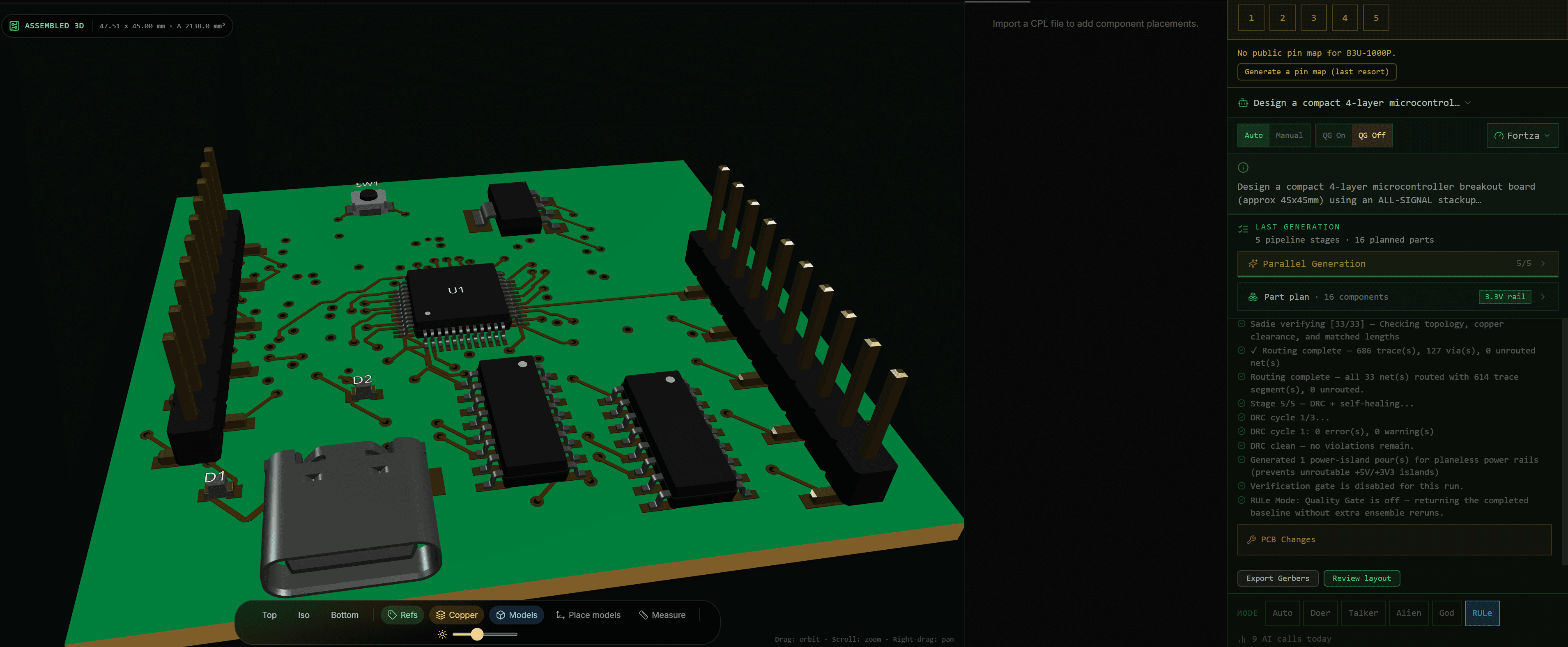
What one prompt produced
Read it critically
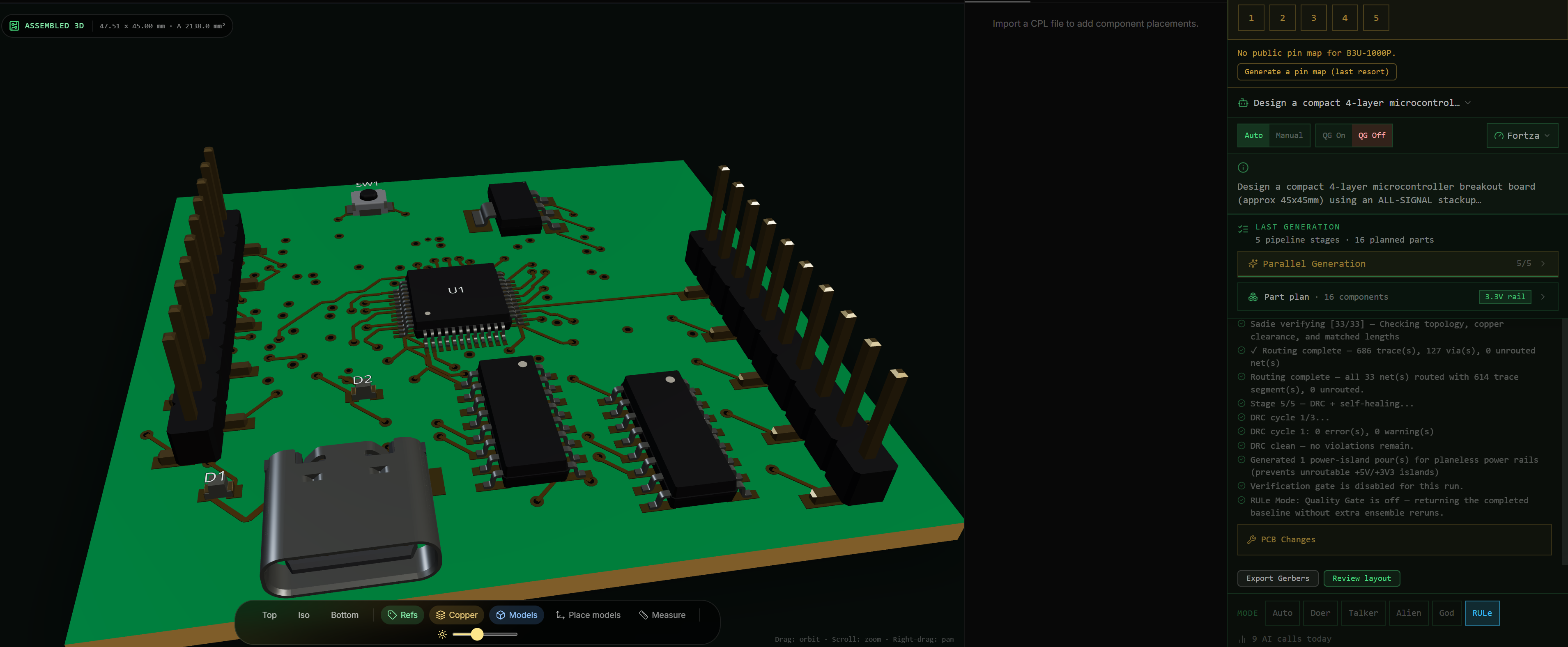
- Quality Gate was switched off for this run (“QG Off” in the panel, and the log says the verification gate was disabled). This is the raw baseline result. The design-rule pass still ran.
- One board is an example, not a guarantee. Dense fine-pitch parts are where you are most likely to see unrouted nets, and every generated board should be reviewed before fabrication.
- The interface has changed since this screenshot was taken. The numbers and the board are what to look at.
Which kind should you pick?
- You already have a finished schematic and need high-speed constraints or self-hosted deployment → Autonomous place and route. PCBEditor vs Quilter
- You lay out in KiCad and want a better front end for schematic capture and sourcing → Schematic automation, or KiCad add-ons. PCBEditor vs ProtoFlow
- You want a rich manual editor with an assistant alongside → An editor copilot. PCBEditor vs Flux.ai
- You need requirement-driven system design with formal engineering reports → Schematic and BoM automation. PCBEditor vs Circuit Mind
- You mainly want to understand a topology or sanity-check a power budget → A chat assistant. What a chat assistant can and cannot do
- You want a first board from a description, in the browser, free, with exportable fab files → Prompt to board. How text to PCB works
Common questions
- What is AI PCB design software?
- Software that uses AI for part of the job of turning a circuit idea into a board a fab can build: choosing parts, writing a schematic or netlist, placing components, routing copper, or checking the rules. Tools differ mainly in how many of those steps they finish. The six kinds above are a map of that spread.
- Can AI design a PCB on its own?
- Partly. AI is good at judgement, such as choosing parts and proposing how they connect. Placement, routing and design-rule checking are measurements, so reliable tools hand them to a deterministic engine. Either way, a person should review the result and confirm it against the fab's capabilities before ordering.
- Is there free AI PCB design software?
- Yes. PCBEditor is free to use in the browser and does not need a credit card. Pricing for other tools changes, so check each vendor's current page rather than trusting a comparison, including this one.
- Will the files work with my fab?
- PCBEditor exports Gerber (RS-274X), Excellon drill, pick-and-place (CPL) and a BOM, plus native KiCad files. Open them in a viewer you trust and check the design rules against your fab's capability sheet before you order.
- How do I tell a working tool from a demo?
- Ask whether the physical result is measured or asserted: real export files, a design-rule check you can re-run elsewhere, and unrouted nets reported by name instead of a completion percentage. The seven-question checklist expands each of those.
Check the output yourself. Describe a board, export the files, open the Gerbers in the free Gerber viewer, and re-run the design rules in a tool you trust.
Try PCBEditor free →