PCB Trace Resistance & Voltage Drop Calculator
Resistance, voltage drop and power loss of a copper trace from its width, length, copper weight and temperature.
- Voltage drop
- 202.1 mV
- Drop as % of supply
- 6.12 %
- Power lost in trace
- 202.1 mW
- Squares (L ÷ W)
- 400.0
- Sheet resistance
- 0.505 mΩ/□
- Copper thickness
- 34.8 µm
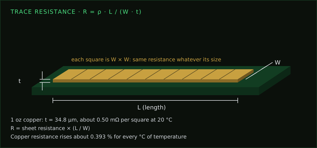
R = ρ(T) · L / (W · t), with ρ(T) = 1.724×10⁻⁸ Ω·m · (1 + 0.00393 · (T − 20 °C)) for annealed copper. Copper thickness t is 34.8 µm per ounce of copper weight.
Voltage drop is R × I; power lost in the trace is I² × R. The result is for the trace alone: vias, connector contacts and solder joints in the same path add their own resistance. Outer-layer plating usually makes finished copper a little thicker than the base foil, so a real outer trace measures slightly lower than this.
The one number worth remembering
1 oz copper has a sheet resistance of about 0.5 mΩ per square at room temperature. A square is any piece of trace as long as it is wide, whatever the size. So a trace 100 mm long and 0.25 mm wide is 400 squares, about 0.2 Ω. The same 100 mm at 1 mm wide is 100 squares, about 50 mΩ. Doubling the copper weight halves both. You can check most power routing in your head with this before you open a calculator.
A worked example: why the 3.3 V rail sags
A 3.3 V regulator feeds a radio module 100 mm away through a 0.25 mm trace on 1 oz copper. The module pulls 1 A in transmit bursts. At 25 °C the trace is about 0.20 Ω, so the module sees about 0.2 V less than the regulator puts out: 6 % of the rail, gone before the module’s own decoupling capacitor. Many 3.3 V parts allow only ±10 % on their supply, and the regulator’s own tolerance uses part of that. Widening the trace to 1 mm brings the drop to about 50 mV (1.5 %); moving the regulator next to the module fixes it outright.
Temperature changes the answer
Copper’s resistance rises about 0.39 % for every degree. A trace that runs at 70 °C inside an enclosure has roughly 20 % more resistance than the same trace on the bench at 20 °C. If the current also heats the trace, the two effects feed each other. Enter the temperature the trace will actually run at, not room temperature. For sizing a trace so it doesn’t overheat in the first place, use the trace width calculator.
What to do when the drop is too high
- Widen the trace, or replace it with a copper pour for the high-current part of the path.
- Use heavier copper: 2 oz halves the resistance of every trace on that layer.
- Shorten the path: put the regulator next to the load instead of next to the connector.
- Run the return path too. Ground current flows back through copper that has resistance as well; a solid ground plane keeps that part small.
- Add vias in parallel where the path changes layer; one small via can be the narrowest point in the route. The via current calculator shows how much each carries.
- For a regulator that supports it, sense the voltage at the load rather than at the regulator, so it corrects for the drop.
What this calculator does not include
It is a DC calculation. At radio frequencies current crowds toward the surface of the copper (skin effect) and the effective resistance is higher; that matters for RF loss, not for supply drop. It also assumes a straight trace of constant width. A neck-down to reach a fine-pitch pad, or a single thin segment in an otherwise wide route, sets the resistance of the whole path more than the wide parts do.
Frequently asked
- What is the resistance of a PCB trace?
- For 1 oz copper it is about 0.5 mΩ per square at 20 °C, where the number of squares is length divided by width. A 50 mm × 0.5 mm trace is 100 squares, about 50 mΩ.
- How do I calculate voltage drop on a PCB trace?
- Multiply the trace resistance by the current. 0.2 Ω carrying 1 A drops 0.2 V. Use the temperature the trace will actually run at, because copper resistance rises about 0.39 % per °C.
- Does 2 oz copper halve the resistance?
- Yes. Resistance is inversely proportional to copper thickness, so 2 oz copper has half the resistance of 1 oz for the same width and length.
- Is trace width calculation the same as resistance calculation?
- No. Trace width calculators (IPC-2221) size a trace so it doesn't heat up too much. This calculator works out how much voltage and power the trace loses. A trace can be cool enough and still drop too much voltage.
- Why does my measured resistance differ?
- Outer layers are plated, so the finished copper is usually thicker than the base foil, and vias, connectors and solder joints add their own resistance. Measure with a four-wire (Kelvin) connection for small values.
Voltage drop is set by how the power net is routed. PCBEditor draws power nets wider than signal nets when it routes, so the drop you just calculated stays where you meant it.
Route power traces at the right width →Related free tools
- PCB Trace Width Calculator (IPC-2221)Minimum copper trace width for a given current + temperature rise, per IPC-2221. Supports internal and external layers, 0.5–3 oz copper.
- Via Current Capacity Calculator (IPC-2152)Max current for a plated-through-hole via, by barrel diameter, plating thickness, and allowed temperature rise.
- Wire Gauge & Ampacity Calculator (AWG)Find the right AWG wire for your current and voltage drop. Includes ampacity lookup and mm² cross-reference.