PCB Trace Spacing vs Voltage Calculator (IPC-2221)
Minimum spacing between conductors at a given voltage from IPC-2221B Table 6-1, for inner layers, bare outer layers and coated outer layers.
- B1: Internal conductors (inner layers)
- 0.10 mm
- B2: External conductors
- 0.60 mm
- B4: External conductors
- 0.13 mm
Values from IPC-2221B Table 6-1 (electrical conductor spacing), in millimetres, for the voltage between the two conductors (DC or AC peak). Above 500 V the per-volt figure is added to the 500 V value: bare outer copper at 1000 V needs 2.5 + 500 × 0.005 = 5 mm.
Columns implemented: B1 inner layers, B2 bare outer layers up to 3050 m altitude, B4 outer layers under a permanent polymer coating. B3 (bare, above 3050 m) and A5–A7 (component leads and terminations) are left out because published reproductions of them disagree; take those from the standard itself. IPC-2221 is a design guideline, not a product safety certification.
IPC-2221 conductor spacing table (mm)
| Voltage (DC or peak) | B1 inner | B2 outer, bare | B4 outer, coated |
|---|---|---|---|
| 0–15 V | 0.05 | 0.10 | 0.05 |
| 16–30 V | 0.05 | 0.10 | 0.05 |
| 31–50 V | 0.10 | 0.60 | 0.13 |
| 51–100 V | 0.10 | 0.60 | 0.13 |
| 101–150 V | 0.20 | 0.60 | 0.40 |
| 151–170 V | 0.20 | 1.25 | 0.40 |
| 171–250 V | 0.20 | 1.25 | 0.40 |
| 251–300 V | 0.20 | 1.25 | 0.40 |
| 301–500 V | 0.25 | 2.50 | 0.80 |
| above 500 V | +0.0025 /V | +0.005 /V | +0.00305 /V |
Use the peak voltage, not the RMS
The table is in DC or AC peak volts. 230 V AC mains peaks at about 325 V, which lands in the 301–500 V band: 2.5 mm between bare outer conductors, not the 1.25 mm the 230 V figure suggests. 120 V AC peaks at about 170 V. Choose “AC, RMS” in the calculator and it converts for you. For the voltage between two conductors, use the largest difference that can appear between them, including transients your circuit is designed to survive.
Below 30 V the table barely matters
At 0–30 V the spacing for bare outer copper is 0.1 mm, finer than most fabs’ minimum gap. On a 5 V or 12 V logic board your fab’s capability, not voltage, sets the clearance. The table starts to drive the layout at 31 V and above, where bare outer copper jumps to 0.6 mm: this is why 48 V motor and PoE boards need wider gaps around their supply nets than the rest of the board.
Does solder mask count as a coating?
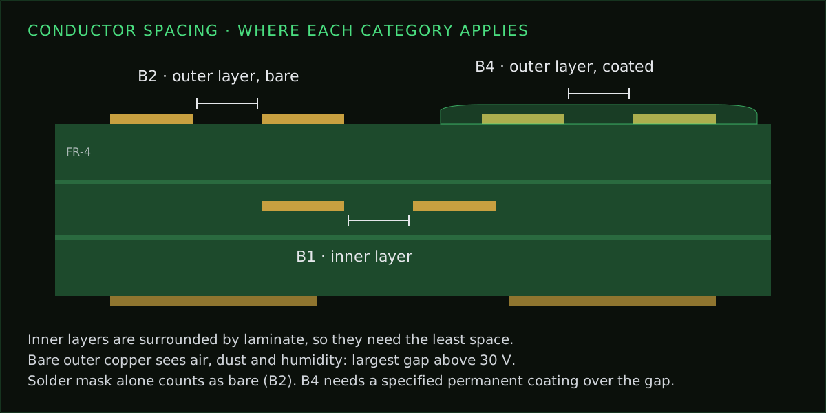
Treat it as bare. Published guidance on IPC-2221 reads the B4 column as a qualified permanent coating over both conductors and the gap between them; solder mask alone is not counted. If you need the smaller B4 gaps, specify a permanent coating and confirm with your fab and your safety standard. The difference is large: at 300 V, bare outer copper needs 1.25 mm and coated copper 0.4 mm.
Clearance, creepage and safety standards
Clearance is the shortest distance through air; creepage is the shortest path along the board surface. Product safety standards, such as IEC 62368-1 for audio, video and IT equipment, set both for mains-connected circuits and between hazardous and touchable parts. Their values depend on pollution degree, material group and insulation type, and are usually larger than IPC-2221. When a board touches mains, design to the safety standard and use this table as a lower bound for everything else on the board.
Getting more spacing on a crowded board
- Move the high-voltage net to an inner layer, where the B1 column applies.
- Cut a slot through the board between the two conductors. It lengthens the creepage path along the surface.
- Pull copper pour back from high-voltage pads; a ground pour is a conductor too.
- Specify a permanent coating if your product and standard allow the B4 values.
- Set a separate clearance rule for the high-voltage net class so the design-rule check enforces it everywhere, not just where you remembered.
Need the values in mils for a fab sheet? Use the mil to mm converter.
Frequently asked
- What is the minimum trace spacing for 48 V?
- IPC-2221B Table 6-1 gives 0.6 mm between bare outer-layer conductors in the 31–50 V band, 0.13 mm with a permanent polymer coating and 0.1 mm on inner layers.
- How much spacing do I need for 230 V AC?
- 230 V AC peaks at about 325 V, which falls in the 301–500 V band: 2.5 mm for bare outer copper per IPC-2221. For mains products, your safety standard's creepage and clearance values apply and are usually larger.
- Is IPC-2221 spacing enough for safety certification?
- No. IPC-2221 is a design guideline. Safety standards such as IEC 62368-1 set creepage and clearance for mains and hazardous voltages, and those are what a certifier checks.
- Does solder mask let me use the coated (B4) values?
- Treat solder mask as bare copper. The B4 column assumes a qualified permanent coating over the conductors and the gap; specify one if you need those values.
- Why are there no A5, A6 and A7 values here?
- Those columns cover component leads and terminations. Public reproductions of them disagree, so rather than risk a wrong safety value this tool leaves them out. Take them from the standard.
A spacing rule only helps if every pair of nets respects it. PCBEditor's design-rule check measures every gap on the board against the clearance you set.
Set clearances for a high-voltage board →Related free tools
- PCB Trace Width Calculator (IPC-2221)Minimum copper trace width for a given current + temperature rise, per IPC-2221. Supports internal and external layers, 0.5–3 oz copper.
- Mil to mm Converter for PCB SpecsConvert mils to millimetres one value at a time or a whole fab capability sheet at once, ready to type into metric design rules.
- PCB Layer Stackup Planner (2/4/6/8-Layer)Plan a PCB layer stack with copper weights, dielectric heights, FR4 Dk values, and finished thickness — 2 to 8 layers.