Via & Through-Hole Pad Size Calculator
Pad diameter, drill size and aspect ratio for vias and through-hole leads, including the diagonal rule for square header pins.
- Pad diameter
- 0.600 mm
- Annular ring each side
- 0.150 mm
- Pad in mils
- 23.6 mil
- Hole in mils
- 11.8 mil
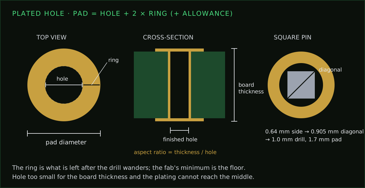
Pad diameter = finished hole + 2 × annular ring + fabrication allowance (the IPC-2221 land-size form). Aspect ratio = board thickness ÷ hole diameter. A square pin must clear its diagonal (side × √2), not its side.
The annular ring and fabrication allowance depend on your fab and your IPC class, so they are inputs here, not built-in constants: take them from your fab’s capability sheet. For component holes the result is rounded up to the next 0.05 mm, the step most fabs drill in. Current capacity is a separate question; see the via current calculator.
Common hole and pad sizes
| Size | Used for | Notes |
|---|---|---|
| 0.4 mm / 0.8 mm | Via (hole / pad) | Roomy via, easy for any fab; good for power |
| 0.3 mm / 0.6 mm | Via (hole / pad) | Common general-purpose via on 1.6 mm boards |
| 0.2 mm / 0.45 mm | Via (hole / pad) | Smaller via for denser routing; check your fab's minimum drill |
| 1.0 mm / 1.7 mm | 0.1 in header (hole / pad) | KiCad's standard 2.54 mm pin-header footprint |
| 0.8 mm / 1.6 mm | Resistor or diode lead (hole / pad) | Typical for 0.5–0.6 mm axial leads |
| 3.2 mm | M3 mounting hole | Clearance hole for an M3 screw |
Typical values seen in common libraries and designs, not a fab specification. Your fab’s minimum drill and minimum annular ring decide what is allowed.
The annular ring is what survives drill wander
Drills don’t land exactly where the file says. The ring of copper around the hole is the margin that keeps the hole inside the pad after it moves. Design the ring larger than the fab’s minimum: if the drill lands off-centre by the full tolerance, the narrow side must still meet the minimum. A ring of 0.15 mm on each side is a common starting point for standard fabs; check yours. Where the pad has to stay small, a teardrop (a widened junction between trace and pad) keeps the connection intact if the hole breaks out on one side.
Aspect ratio: why tiny holes in thick boards fail
Plating has to flow down the hole to coat the wall. When the hole is narrow compared with the board thickness, the middle of the barrel ends up thin. Fabs publish a maximum aspect ratio for through-holes; around 8:1 to 10:1 is common for standard processes. A 1.6 mm board at 8:1 needs a hole of at least 0.2 mm. Smaller vias on a thick board mean a thinner board, laser-drilled microvias or a fab with a tighter process.
Square header pins: size the hole for the diagonal
A standard 0.1 in header pin is 0.64 mm square, so its corner-to-corner diagonal is about 0.905 mm. A 0.9 mm hole looks right on paper and the pin will not go in. KiCad’s standard 2.54 mm header footprint uses a 1.0 mm drill and a 1.7 mm pad; the large ring (0.35 mm) gives hand soldering something to hold. The calculator rounds up to the next 0.05 mm, so with a 0.1 mm clearance it suggests 1.05 mm, a little looser than KiCad’s 1.0 mm; both are standard drill sizes.
Round leads and through-hole parts
Use the maximum lead diameter from the datasheet, not the nominal, and add clearance: roughly 0.15 to 0.25 mm for machine insertion and wave soldering, more for parts you will fit by hand. Too tight and leads won’t insert; too loose and solder can’t bridge the gap reliably. If you need the whole footprint, not just the hole, the footprint generator builds one from datasheet dimensions.
Frequently asked
- What is a standard via size?
- A 0.3 mm hole with a 0.6 mm pad is a common general-purpose via on a 1.6 mm board. Smaller vias such as 0.2 mm / 0.45 mm suit denser routing if your fab supports the drill.
- How do I calculate pad size from hole size?
- Pad = finished hole + 2 × annular ring + fabrication allowance. A 0.3 mm hole with a 0.15 mm ring and no extra allowance gives a 0.6 mm pad.
- What hole size for 0.1 inch header pins?
- Size it for the pin's diagonal, about 0.905 mm for a 0.64 mm square pin. KiCad's standard header footprint uses a 1.0 mm drill and a 1.7 mm pad.
- What is the minimum annular ring?
- It depends on your fab and your IPC class. Take the minimum from your fab's capability sheet and design a little larger so the ring survives drill tolerance.
- What is PCB aspect ratio?
- Board thickness divided by hole diameter. Fabs set a maximum, commonly around 8:1 to 10:1 for standard through-holes, because plating struggles to reach the middle of a narrow hole.
Hole and pad sizes become via classes in PCBEditor. The design-rule check then flags any drill or ring that falls below your fab's limits.
Design a board with these hole sizes →Related free tools
- Via Current Capacity Calculator (IPC-2152)Max current for a plated-through-hole via, by barrel diameter, plating thickness, and allowed temperature rise.
- PCB Layer Stackup Planner (2/4/6/8-Layer)Plan a PCB layer stack with copper weights, dielectric heights, FR4 Dk values, and finished thickness — 2 to 8 layers.
- IPC-7351 Footprint Generator (KiCad)Generate an IPC-7351 compliant PCB footprint from body/pad dimensions. Downloads as a KiCad `.kicad_mod` file. No AI, no upload, no signup.